By Jean-Jacques DeLisle, contributing writer
Several chipmakers are developing new memory storage technologies that will change the way that data is stored. These are enhancements of NAND flash memory that can store information faster, in a smaller space, and with less power consumption than previous generations of product. Demand for more powerful and compact storage technology is growing as more and more information is being stored in the cloud and new technologies such as artificial intelligence (AI) programs and computer-assisted engineering (CAE) are becoming more prevalent.
Here’s a look at some recent developments in the memory and storage device markets.
Samsung Electronics, one of the leading developers of advanced memory technology, recently announced its fifth-generation V-NAND memory chips. The new V-NAND chips claim the fastest data transfers and the industry’s first use of the Toggle DDR4.0 interface. With data speeds as high as 1.4 gigabits per second (Gbits/s), the 256-Gbit V-NAND chips are 40% faster than the previous 64-layer product.
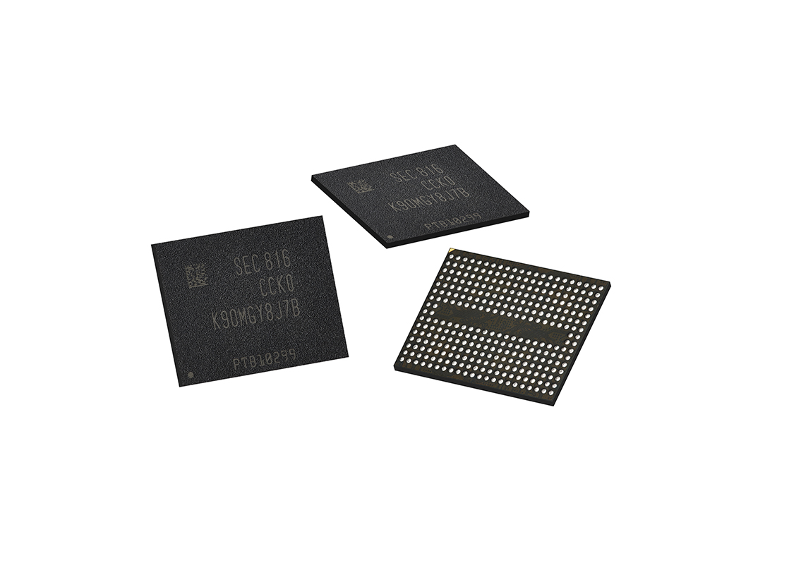
This increase in speed is not at the expense of energy efficiency, however. The V-NAND chips offer comparable efficiency to the previous 64-layer chips. Samsung accomplished this by lowering the operating voltage of the chips from 1.8 V to 1.2 V. The new chip also claims the fastest write speed, clocking in at 500 microseconds (µs). This improvement represents about a 30% increase over the previous generation. In addition, the response time to read signals has been reduced to 50 µs.
The secret to these new chips is in their structural design. Inside the V-NAND chips are more than 90 different layers of 3D charge trap flash (CTF) cells. The cells are arranged in a pyramid structure with tiny channel holes carved vertically throughout, said Samsung. The holes are only a few hundred nanometers wide, and within these holes are housed more than 85 CTF cells that can each store 3 bits of data.
Samsung said that this state-of-the-art memory fabrication is the result of several breakthroughs that include advanced circuit designs and new process technologies. The company has started mass production of the fifth-generation V-NAND and expects to quickly ramp up production.
While Samsung is developing cutting-edge memory chips on its own, other companies are teaming up to develop faster and smaller memory as well. Micron Technology Inc. and Intel Corp. are working together on a joint development program known as 3D XPoint, which aims to develop new, faster, and more powerful memory chips for data centers. The partnership has resulted in a new classification of memory chip that exhibits lower latency and far greater endurance than traditional NAND memory chips, said the companies.
The partnership recently announced that it will complete the development of the second generation of 3D Xpoint technology, which is expected in the first half of 2019. Each company will independently pursue the development of the technology after the second generation. They will continue to manufacture memory based on 3D Xpoint technology at the Intel–Micron Flash Technologies (IMFT) facility in Lehi, Utah.
Micron and Intel also announced the production of the industry’s first 4-bits/cell 3D NAND technology, leveraging the 64-layer structure to achieve 1 terabit density per die, the highest-density flash memory. They are also progressing on the third-generation 96-tier 3D NAND structure, a 50% increase in layers.
Independently, Micron announced in May the release of its first solid-state device (SSD) built on its quad-level cell (QLC) NAND technology. The Micron 5210 ION SSD provides 33% more bit density than triple-level cell (TLC) NAND. Micron’s QLC NAND reaches densities of 1 terabit with its next-generation 64-layer 3D NAND structure.
Other companies are also getting in on the action. As information storage demand grows, so does the number of companies fighting for memory superiority. Late last year, SK Hynix Inc. claimed the industry’s first 72-layer 256-Gbit 3D NAND flash chips, built on its TLC arrays. The company said that it stacks one-and-a-half times more cells for the 72-layer 3D NAND than the previous 48-layer 3D, achieving 30% more manufacturing productivity. Thanks to high-speed circuit design, the new memory chip also delivers two-times-faster internal operation speed and 20% higher read/write performance than the 48-layer chip.
Advertisement
Learn more about Electronic Products Magazine


