Cameras are everywhere, and users increasingly expect more from their optical imaging sensors. CCD sensor technology hasn’t fundamentally changed in recent years, but CMOS technologies have. Mobile, automotive, and emerging markets drive these changes as little by little, more markets convert from CCD to CMOS, and new markets emerge that are only feasible with CMOS sensors.
Technology drivers
Radhika Arora, Sr. Segment Marketing Manager at Aptina Imaging Corporation, says the CMOS image sensor market is growing at a 10% to 12% CAGR, and integration into mobile devices was responsible for 65% of that in 2013. An example of a fast growing segment within the mobile market is tablets, which typically have one or two optical sensors in each device. Arora expects the quickly growing mobile market will reach $1.5B by 2017.
Andrew Burt, VP of the Image Sensor Business Unit of Toshiba America says the smartphone arena is extremely tough right now. “As the camera function is turning into a commodity, there are huge price pressures driving sensor designs.”
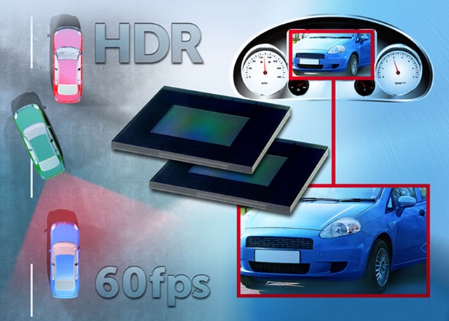
The automotive market is also driving CMOS sensor technologies as manufacturers are pushed by regulations for greater safety. Toshiba recently addressed this market with a special-purpose imager (see Fig. 1 ), and today one can find as many as 14 cameras in each vehicle. Forward- and rear-looking cameras on both sides for collision avoidance and back-up warnings, wing mirror cameras that view the road, and multiple in-cabin cameras have different sensor needs and design motivations from those used in mobile markets, Arora explains. In mobile cameras, higher-resolution sensors are perceived as being better, but in automobiles, high-performance and special features, like high dynamic range (HDR) and infra-red (IR) for in-cabin sensing and low-light performance, drive sensor design and resolution requirements. Arora says Aptina has a dominant position delivering CMOS image sensors in the automotive space for more than 10 years.

Fig. 1: In new car models, Toshiba's ultra-compact CMOS i mage sensor will drive smaller camera modules in parking-assist systems, surround-view systems, and side-view systems.
Emerging markets are the next largest growth area for CMOS sensors, involving traditional sectors such as machine vision, security/surveillance, and medical applications, which are “high value” fields, as opposed to “high volume” fields like mobile devices. In the large surveillance market, CMOS image sensors monitor municipal city activities, and are in ATM cameras, video door bells, and new video locks with facial recognition. Wearable electronic devices like those that dominated the headlines at the 2014 CES, such as gesture control, and 3D glasses are other examples.
Arora says the shift from CCDs to CMOS is positively impacting the medical field. CMOS image sensors are driving down the cost of devices like endoscopes and are also lowering their power and sizes, which can increase patient comfort. Another area of growth for CMOS image sensors is the $100 disposable DNA sequencer, which can address the high cost of gene sequencing.
Are CCDs dead?
Toshiba is unique in the image sensor industry because it has made both CMOS sensors for 10 to 12 years, and CCD sensors for 25. Burt says, “From a volume viewpoint, CMOS is winning hands down, and its deployment is ever increasing. We see stagnation and are possibly on the edge of the decline of the CCD. They still have some benefits in more robust areas where the product will be bounced around, but CMOS technology is proving to be great in some of those markets too, like automotive.”
CCD sensors are still used in applications with higher supply voltages, like machine vision, all-in-one scanners and printers, and bar code readers. Joost Seijnaeve, product marketing manager at ON Semiconductor’s CMOS sensor division, says “Right now, CCDs have 40% to 50% of the sensor market. But, in two years it will shrink to 20% because the quality of CMOS sensors has improved.”
Fundamental shifts
Early CMOS imaging sensors suffered from poor quality because they had inferior light sensitivity compared to CCDs. Foundries added passive and active diodes to standard CMOS technologies. Then they created pixels with buried diodes, which is what is done in CCDs. Seijnaeve explains that diodes deeper in the silicon material have fewer crystal defects and significantly reduced dark current compared to diodes located on a wafer’s surface where most defects lie. Later they added amplifiers and A/D converters, which still cost less than CCDs.
Over the last 5 to 6 years, CMOS sensors have shifted toward backside illumination (BSI), where the back of the sensor wafer is ground extremely flat and light shines in through that side, effectively producing upside-down pixels. Toshiba first implemented BSI in production around 2009, but now almost all sensor companies support it. Burt says 50% of the total CMOS sensor sales in 2013 used BSI, and by 2018, more than 70% will.
Manufacturers have also raced toward smaller pixels to provide cameras with higher pixel counts and resolution. But this hasn’t meant better image quality. Shrinking the pixel size decreases the photon collection area and light capacity, so there is less dynamic range. Fundamentally new design innovations are needed to achieve both higher pixel densities and high sensitivity.
Arora says Aptina is offering new pixel designs that address these shifts. Clarity+ technology is one example that replaces the green pixel in the RGB color filter with a clear pixel. This doubles the sensor’s low-light sensitivity and increases color accuracy and detail. Aptina initially offered it for the mobile market and will introduce it to other market segments.
More CMOS sensors now include high dynamic range (HDR) technologies that allow a camera to operate in low and high light environments (see Fig. 2 ). Each sensor manufacturer has a proprietary strategy. Burt says almost every sensor for the mobile market has some sort of HDR capability, and it’s becoming the expectation. But, according to Seijnaeve, requirements determined by the automotive and security markets, where it is important that the sensor immediately adapts to high-contrast light and dark situations, are driving this technological trend.
“Users want to be able to see when driving into a dark tunnel and again into the light. In our sensors today, there are some CMOS operation modes that increase the dynamic range, but it is still a domain with lots of investigation and research. There is no simple technique that gives very high dynamic range,” Seijnaeve says.


Fig. 2: In an image captured without HDR (top), critical information is lost. With HDR (bottom), it is clearly visible.
Deploying new technologies on a CMOS sensor so it can cooperate with a coprocessor, like in smart phones, is another new shift. Toshiba’s new Bright Mode technology uses a novel patented Electronic Dispersion Compensation (EDC) strategy that deals with data read in from each pixel at extremely high frame rates, such as 300 fps, and allows playback at much lower speeds, like 15 fps, providing an extremely detailed visual playback experience. Toshiba demonstrated this technology in a mobile phone at CES2014, and Burt says Toshiba is working with OEMs to get products on the market in 2015.
Technical issues to overcome
99.99% of mobile camera sensors have active pixels with a rolling shutter that was optimized for cost and performance. A rolling shutter operates like a curtain that rolls over different pixels at different times and is the simplest and cheapest device to get pretty good noise performance. But they deform images in motion and have motion blur that can’t be corrected.
Global shutters are needed when imaging objects that move at high speeds, such as optical scanning and machine vision applications. They are like electronic versions of mechanical shutters that expose all pixels to light at the same time.
Many manufacturers are looking into integrating global shutters with CMOS sensors since users prefer them, but there are tradeoffs. One is the cost associated with the extra memory they require, making them too expensive for some cost-sensitive applications like mobile devices. Another is noise performance.
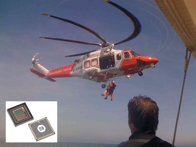
Seijnaeve says it’s not yet feasible to make global shutters in CMOS with the low noise performance of a rolling shutter. If applications need very low noise, they use CCD sensors with global shutters, but they’re expensive. A 1.3megapixel full-frame transfer noise performance CCD costs about $300, and the new 1.3 Python CMOS sensor from ON Semiconductor with a global shutter as seen in Fig. 3 is about $50. It’s hard to make commercial cameras at high volume with CCDs, but the CMOS sensors have promise.

Fig. 3: The Python 1300, ON Semiconductor's latest CMOS image sensor (inset), has a global shutter for capturing images at high speeds. This can eliminate the distortion of the fast moving helicopter blades seen in the accompanying photo.
Advertisement
Learn more about AptinaON SemiconductorToshiba America Electronic Components


