New packaging, MOSFETs meet power supply needs
The drive for more power in tighter dimensions is addressed by advancements in both Si and packaging technologies
BY JEFF SHERMAN
Texas Instruments
Dallas, TX
http://www.ti.com
The drive for more power in tighter dimensions is being addressed by advancements in both silicon and packaging technologies. A new power MOSFET combines a new generation of silicon technology with a package that allows topside cooling in a standard footprint. This combination enables new levels of efficiency, power density and reliability to be achieved.
Power designers are consistently faced with more challenging designs because of advanced processor requirements and increasing features. Board space allocated to the power conversion is usually being reduced, even though demands in terms of number of power rails and actual output power are increasing. Advanced packaging options like the DualCool NexFET power MOSFET help designers meet these demands in a standard footprint. Combining the NexFET power MOSFET that enables high-frequency operation by reducing switching losses and the DualCool power package with its top-side cooling capability results in significantly higher power density.
Ideal switch
The major losses that occur within a MOSFET switch in a typical synchronous buck converter consist of switching, conduction, body diode and gate drive losses. The switching losses are primarily caused by the parasitic capacitances formed within the structure of the device. The conduction losses are a result of the device’s resistance (RDS(on) ) when it is in enhanced-mode operation. Body diode losses are a function of its forward voltage and reverse recovery (Qrr). Gate drive losses are determined by the MOSFET’s Qg. Therefore, the parasitic capacitances and the RDS(on) determine the device’s performance in a specific application. The most common technology used in today’s low-voltage MOSFETs is the TrenchFET (see Fig. 1 ).

Fig. 1. MOSFET structure comparison.
The TrenchFET’s claim to fame is its ability to achieve ultra-low resistance for a specific die size over the planar technology that it replaced. Its only negative aspect is that the parasitic capacitances actually increase. The large area of the trench walls makes it difficult to keep the internal capacitances small. The resulting high capacitances force designers to choose between a low operating frequency to optimize the efficiency and high frequency with better power density.
The NexFET can achieve similar specific on resistance to the TrenchFET technology while reducing the associated parasitic capacitances by about fifty percent. The device finds its roots in a laterally defused MOS (LDMOS) and combines vertical current flow to achieve high current density. A closer look at the structure (see Fig. 1 ) reveals that the area underneath the gate has minimum overlap over source and drain regions, keeping the internal capacitances small. The reduced capacitances result in lower charges (Qg , Qgs , Qgd ) required to switch the device. Therefore, the device switches faster, reducing switching losses within the MOSFET. Also, less energy is required from the drive circuit, reducing the losses in the driver. The Miller charge (Qgd ) within the device impacts the device’s switching losses as well as determines the switch’s ability to avoid C dv/dt turn on, which can further reduce efficiency and potentially damage the MOSFETs.
The net effect of the NexFET technology improvements is it lowers and flattens the power loss curve versus frequency (see Fig. 2 ). Therefore, the typical synchronous buck converter can operate at twice the frequency while maintaining the same power loss. If, for example, we limit our power loss to 3 W to maintain full-load efficiency above 90%, the switching frequency can be increased from 500 kHz to 1 MHz, versus state-of-the-art Trench MOSFETs. At higher frequencies, passive components like the output inductor can be reduced in size by up to 50% to improve power density.
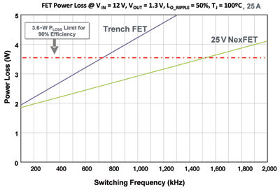
Fig. 2. The new power MOSFET flattens power loss curve enabling higher frequency.
The ideal package
The semiconductor device has limitations in terms of its ability to improve power density. Power dissipation within the device still needs to be managed to minimize its impact on board area and thermal interaction between components.
Figure 3 shows a cross-sectional view of the DualCool package versus a standard QFN package. The package outlines are shown between a printed-circuit board (PCB) and a heat sink. The footprint of the two packages is identical, making it easy for a designer to use either package without board modification. In both packages, the silicon die (shown in red) is mounted on the package leadframe and a copper clip is used to connect the top of the die to the source pin on the right side. Alternatively, the DualCool package uses a metal slug to extend the source of the device to the top of the package. This reduces the thermal impedance from the silicon junction to the top-side (RθJT ) from approximately 10C/W in the standard QFN to 1.2C/W. This means the thermal resistance to the top side is roughly equivalent to that of the bottom side. The top of the heat slug must be flush, avoiding any non-coplanarities with the package, and is both a thermal and electrically active connection. Therefore, an insulator must be placed between the package and the heat sink.
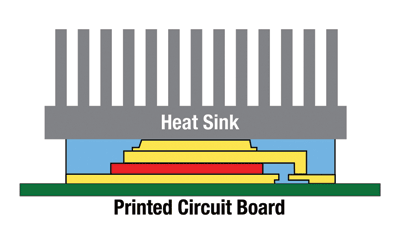
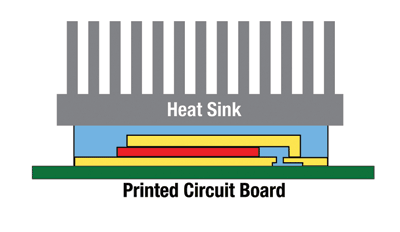
Fig. 3. Cross-sectional view of DualCool (top) and standard QFN packages (bottom).
When the DualCool package is combined with a heat sink, the heat can be pulled away from the PCB through natural or forced convection cooling and transferred into free air. This allows the package to dissipate up to 80% more power than the standard QFN package, based on system level simulations (see Fig. 4 ).
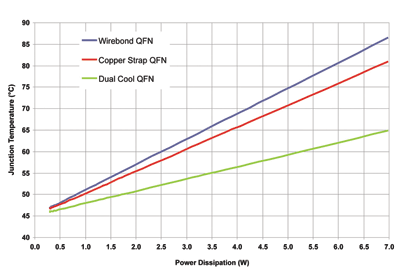
Fig. 4. Up to 80% more power dissipation capability in the new package.
Higher power dissipation can be used to provide up to 50% more current to the load. Thus, enabling the designer to increase output power and improve the power density while maintaining the same junction temperature. Alternatively, the circuit can provide less than a 50% increase in current and operate at a lower temperature, minimizing the heat’s impact on other components and improving system reliability. ■
Advertisement
Learn more about Texas Instruments


