New power semiconductors cut data center energy
Advanced MOSFETs and diodes aid efficiency
BY STEVEN SAPP, RITU SODHI, and SAMPAT SHEKHAWAT
Fairchild Semiconductor
San Jose, CA, Pune, India, and Mountaintop, PA
http://www.fairchildsemi.com
The vast arrays of computers around the world consume huge amounts of power. Data centers that enable the Internet exemplify this power usage. As much as 1.2% of the power consumed in the entire U.S. is taken by servers. Worldwide, in 2005 more than $7 billion dollars was spent on powering servers and the infrastructure supporting them requiring the equivalent capacity of fourteen 1,000-MW power-generating facilities.
There is waste associated with power conversion and conditioning, distribution, and environmental control. In a typical data center, less than half of the power consumption goes into the computing function. Data center operators look at every opportunity to increase power conversion and distribution efficiency including cutting the number of conversion stages through the distribution of high-voltage direct-current sources (see Fig. 1 ).
In the U.S., the electric grid distributes ac power to local communities at around 13,800 Vac. That is eventually stepped-down to 480 Vac using transformers that do not contribute significantly to energy loss.
The data centers almost always have an uninterruptible power supply, commonly a double-conversion online UPS. This stage of the power conditioning may be only 70% efficient. At the server rack the 208-Vac power is converted to 12 or 48 Vdc and later stepped down to the bus voltages for the processor, disk drives, and memory. These items benefit from high-performance semiconductor components like IGBTs and Super-Junction power MOSFETs for rectification, battery charging, and dc/ac inverting.

Fig. 1. Power conversion stages in a typical data center.
A fully populated server rack with two processors per board could use 5 kW and waste as much as 500 W with 90% converter efficiency. High-performance low-voltage MOSFETs have enabled improved efficiency for these conversion stages with both lower on-state resistance and lower switching loss. In the last decade, VREG efficiency has increased by more than 5% and output current rating has increased by five times. Buck converters of past generations used a Shottky diode and a 60-V-rated power MOSFET, achieving 80% to 85% efficiency. Even though processor input voltage has decreased, present power MOSFET products can achieve greater than 90% efficiency.
Advanced LV power MOSFETs
Until the mid 1990s, the focus of development in low-voltage power MOSFETs was the RDS(on) as conduction losses were the dominant components of the total power loss. As switching frequencies started to go up, researchers started to look at gate capacitance and gate charge more closely. Figure 2 shows trends in the figure-of-merit for power MOSFETs – normalized RSP and combined RSP •Qgd. There has been close to a 10X reduction in these features over the last 14 years.
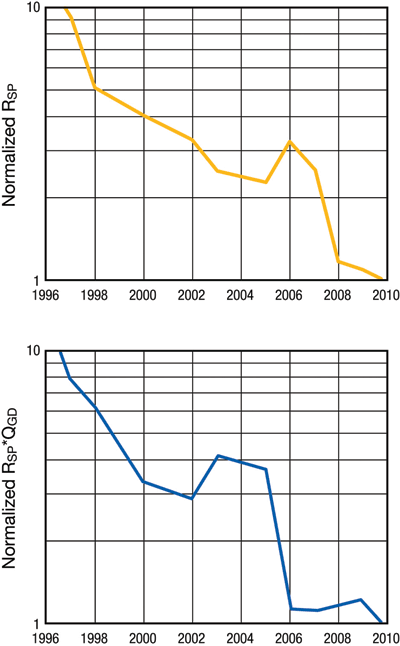
Fig. 2. Figure-of-merit trends for a 30-V power MOSFET over time.
Several new technologies have been developed to reduce both on-resistance and gate charge. One of these was the incorporation of a thicker oxide at the bottom of the gate trench (see Fig. 3 ). This helps reduce the Cgd, and improves drift region resistance. It also helps to decouple the on-resistance and gate charge, because now one can keep a thin gate oxide to get lower VTH , and hence lower on-resistance, but at the same time have a thicker trench bottom oxide to give the lowest capacitance, Cgd.
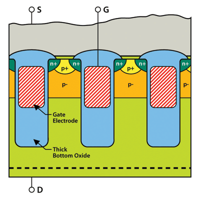
Fig. 3. Device cross-section of a power MOSFET with thick bottom oxide.
Another concept that was originally developed for high voltage devices is the use of charge balance or Super-Junction device structures. With this approach, one can obtain two-dimensional charge coupling in the drift region. This enables the use of higher doping in the drift region and reduced drift resistance. At Fairchild, this concept has been implemented using a fourth electrode, shield, and a thick oxide (see Fig. 4 ).
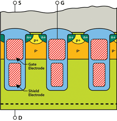
Fig. 4. Device cross-section of a power MOSFET with shield electrode.
Other parameters are now becoming more relevant, such as the body diode reverse recovery, internal gate resistance, and the MOSFET output charge (Qoss ). Low-voltage MOSFET products are being optimized to minimize the diode reverse recovery and the output capacitance. The package’s resistance, inductance, and thermal properties also play a key role in determining the power loss, especially as the devices are becoming smaller in size and co-packaged solutions gain a foothold in the application.
In a dc/dc converter application, while on-resistance controls the high load efficiency, the gate charge, reverse-recovery charge, and output capacitance control the light load efficiency. Figure 5 shows the relative power loss of various components at different output loads.
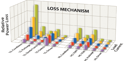
Fig. 5. Relative contribution from various power-loss components in a dc/dc converter.
The pace of development of power conversion silicon solutions may have accelerated in recent years. Efficiency gains, particularly at light load conditions, are expected to advance significantly for devices targeted for introduction in 2010 (see Fig. 6 ).
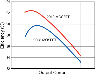
Fig. 6. Efficiency comparison between two generations of power MOSFET technology.
Advanced high-voltage devices cut losses in the ac/dc stage
Switch-mode power supplies with PFC are used in the first power conversion stage in data centers; and now in telecom power supplies and white goods. Historically, power factor correction circuits have used a boost converter topology that combined a power switch (MOSFET or IGBT) and boost diode. However, with the introduction of the soft recovery diode, like Fairchild Semiconductor’s Hyperfast Stealth, snubber circuitry may be eliminated or reduced and the boost converter can be implemented in the hard-switched mode. When the Stealth diode or SiC Schottky diode is combined with new Super-Junction technology like SupreMOS, designers can obtain lower conduction and switching losses, simplified gate drive, and reduced EMI.
Using PFC not only ensures compliance with regulatory specifications such as EN61000-3-2 for reduced harmonic content and improves reliability due to less stress on components, it also improves efficiency by increasing the maximum power that can be drawn from the source.
Most high-power active PFC designs for an ac/dc stage incorporate a continuous current mode (CCM) boost converter topology because of its simplicity and wide ac input voltage range. Another PFC operating mode, boundary conduction mode (BCM), is used at low power levels. The CCM boost converter operates the boost diode and switching device in the hard-switched mode, where diode reverse-recovery characteristics increase the switching device’s turn-on losses and the generated EMI.
The diode’s reverse-recovery characteristics determine how it transitions from the forward conducting state to the reverse voltage blocking state. If the return of the reverse recovery current from IRRM to zero is too abrupt, voltage spikes and severe EMI are generated. To soften this response, designers have either slowed down the switch turn-on di/dt and/or added snubber circuits. With prior diode technology, the designer was limited to having either a soft or fast diode. The large IRMM value of previous soft diode technology generated high turn-on loss during the diode tRR period.
At the same time, slowing down the switch turn-on increases the loss. Adding snubber circuitry adds cost and complexity and reduces reliability. Besides, the snubber circuits often involve complex energy recovery schemes, since the basic RC approach results in high power dissipation in the snubber resistor. To overcome this problem, a Stealth II diode can reduce turn-on loss. MOSFET Super–Junction technology can have extremely low RDS(on) to reduce conduction loss and the Super-Junction device can be extremely fast, cutting turn-off loss. ■
Advertisement
Learn more about Fairchild Semiconductor


