Do you want higher bandwidth without sacrificing the speed or limit of your data transfers? Well, you may not know it, but what you really want are plasmonics.
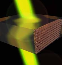
What are those, you ask? Plasmonic technology is a very, very recently developed technology that seeks to combine the very best parts of optical and electronic data transfers and eliminate the worst, by crowding light into metal structures so data can be transmitted at much, much higher frequencies—and therefore, can help you get higher bandwidth and faster data transfers.

Plasmonic technology crowds light into metal for faster data transmissions
Expanding on this principle, scientists at the Univesity of Utah have managed to create a technique that produces plasmonic technology through the use of electrical conductivity. Published by Advanced Optical Materials on March 7, the technology in their study could potentially create much faster electronic components, print magnetic materials, and make wireless technology faster.
Plasmonics “crowd” light into metal structures with dimensions much smaller than that light’s wavelength, allowing data to be transmitted through terahertz frequencies. As we know, terahertz frequencies lie in the middle of microwave and infrared light on the electromagnetic radiation spectrum—much faster than the speed data is currently transmitted.
Led by electrical and computer engineering professor Ajay Nahata, the University of Utah group has developed a way to create a “low-cost, widely applicable way to make plasmonic materials,” something that means big things for the tech world as current plasmonic arrays can only be created one at a time through expensive microfabrication equipment.

The team used a commercially available inkjet printer along with one silver and one carbon ink color cartridge in order to print 10 different plasmonic structures on 2.5 x 2.5-inch plastic sheets. Each structure came with a periodic array of 2,500 different-sized holes and spacing, which allow researchers to control the array’s electronic conductivity—how effective the structure could carry an electrical current. The study then tested four separate arrays with holes 450 microns in diameter, which is only about four times the width of a single human hair. When the group varied the amounts of silver and carbon ink they used, they were able to control the plasmonics electrical conductivity.
According to Nahata, this allows users to “make rapid changes to the plasmonic properties of the metal, without the million-dollar instrumentation.”
What all of this means is that engineers could use this new printing technique to create wireless devices that transmit data much more quickly than we’re used to, which is certainly something to be excited over. Additionally, the technique could eventually produce more compact magnetic materials with a bit of fine-tuning, though according to Nahata that’s not likely to happen for at the very least five more years. But all in all, plasmonic technology? Pretty cool. Now you know.
SourceEurekaAlert
Advertisement


