By Maurizio Di Paolo Emilio, editor, Power Electronics News
The growing demand for technology in electric vehicles, telecommunications, and industrial applications has led Soitec and Applied Materials to form a joint development program for next-generation silicon carbide (SiC) substrates for power devices. The program aims to provide technology and products to improve the performance and availability of SiC devices for the next generation of e-mobility.
“We look forward to working closely with Soitec to create materials engineering innovations for silicon carbide technology,” said Steve Ghanayem, senior vice-president of new markets and alliances at Applied Materials.
OEMs who design with power devices of course want the most efficent products they can get, and improved efficiency is possible when using III-V semiconductors (including SiC) instead of silicon. SiC significantly reduces power losses and enables higher power density, voltages, temperatures, and frequencies while reducing heat dissipation. SiC also has a bandgap about 3 times wider, and a distance of the drift region that can be reduced to about one-tenth with the same breakdown voltage.
“High-voltage SiC devices offer an attractive combination of fast switching and low losses, giving application users unprecedented levels of flexibility in the choice of topology for medium- and high-voltage power conversion.” Said Olivier Bonnin, compound business unit general manager at Soitec.
But there are factors impeding the rapid transition to silicon carbide substrates.
“Higher quality SiC materials are needed to increase yield (lower defect density) and reliability. Improvements in wafer planarity are required to accommodate processing in high volume foundries and reduce processing costs,” said Bonnin.
The future of electric mobility will be based on technological innovations starting from the level of semiconductor materials and substrates. Demand has been rising for SiC-based semiconductor materials over the past year.
Bonnin quoted statistics from Yole Developpement that the SiC power device market will grow from $560 million today to $2 billion in 2024, which represents a CAGR of 28 percent. “SiC will likely be the material of choice for the next ten years,” said Bonnin.
The goal of the technology development program with Applied Materials is to create samples of SiC engineered substrates within the second half of 2020, based on Soitec's proprietary Smart Cut technology. Smart Cut technology is currently in use for the manufacture of silicon-on-insulator (SOI) products widely adopted by chip manufacturers.
“Soitec’s technologies aim to address those challenges through the layer transfer of best in class quality SiC materials on specific receivers, together with multiple recycling of the SiC materials,” said Bonnin.
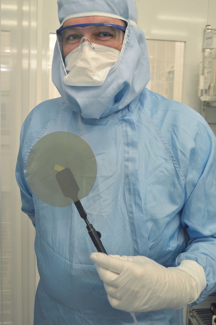
“Smart Cut is our wafer-bonding and layer-splitting technology. Essentially, it is a method for turning a single high-quality SiC wafer into multiple high-quality SiC wafers. It achieves this by removing a very thin layer of crystalline material from a high-quality donor substrate and bonding it to a wafer of lesser cost/quality. This results in multiple wafers with high-quality surfaces upon which semiconductor devices can be built. We believe that our Smart Cut technology is applicable to SiC where it can enable significant improvements at the substrate and device level in quality, performance, and costs (Fig. 1).” Said Olivier.

Fig. 1: Soitec employee with Smart Cut-based SiC wafer (Image: Soitec)
The switching and conduction losses per chip will be significantly reduced, but the chip area will be reduced even more with a high power density that will have to cope with efficient thermal management.
One of the earliest wide bandgap (WBG) devices to enter the marketplace is a SiC power diode, with broad penetration into specific sectors including PV converters and motor drives. These devices offer immediate improvements in efficiency, higher voltages, and thermal behavior. The material’s intrinsic performance enables those benefits: SiC has a room temperature thermal conductivity above 300 W/mK.
“Our technology will take advantage of the SiC materials properties together with the possibility to push its benefits up to new devices challenges thanks to some specific layer engineering,” said Bonnin.
Temperature factors and switching frequency are essential elements in an e-mobility design. The stability at high temperatures and the operability at a higher switching frequency compared to its partners Si, involves a reduction in the size and weight of the system as components replace the bulky magnetic components with a lower form factor.
The electrical challenges will resolve the problems of current leakage in the switching mode, which can cause overvoltages and significant oscillations. These problems can be avoided thanks to circuit layouts for controlling the current flow in the vicinity of the power module.
Another problem is related to the capacitive coupling between the alternating current and the earth: this coupling becomes critical as it generates significant electromagnetic interference. Also, in this case, the intelligent design of the power module can help reduce this effect.
The cost is obviously an element to consider: the biggest challenge is the wide adoption of SiC devices. The electrical characteristics show how they can lead to significant reductions in system costs, but above all, to a real increase in overall efficiency. SiC devices will change the application game with new packaging techniques.
The article originally published at sister publication EE Times.
Advertisement
Learn more about Electronic Products Magazine


