By Jean-Jacques DeLisle, contributing writer
Gallium-nitride (GaN) power transistors have become an efficient and robust solution for modern power electronics for household and low-power industrial applications. The nature of GaN transistors’ higher-voltage capabilities and efficient operations have made them attractive alternatives compared to silicon or other technologies. However, commercially available GaN devices have yet to reach high-enough operating voltages to be used in power-grid applications or other high-voltage applications. This may all change, as researchers with MIT, Columbia University, the Singapore-MIT Alliance for Research and Technology, IQE, and IBM have recently developed GaN transistors that are able to exceed commercial voltage levels of 600 V and reach 1,200-V operating range. Though there has been substantial research attempting to create higher-voltage GaN transistors, neither the traditional lateral style of transistors or variants of vertical, or fin, transistors have yet to be viable with commercial transistor fabrication techniques.
“All the devices that are commercially available are what are called lateral devices,” said Tomás Palacios, MIT professor of electrical engineering and computer science. “So the entire device is fabricated on the top surface of the gallium-nitride wafer, which is good for low-power applications like the laptop charger. But for medium- and high-power applications, vertical devices are much better. These are devices where the current, instead of flowing through the surface of the semiconductor, flows through the wafer across the semiconductor.” According to Palacios, vertical devices are much better in terms of how much voltage they can manage and how much current they control.

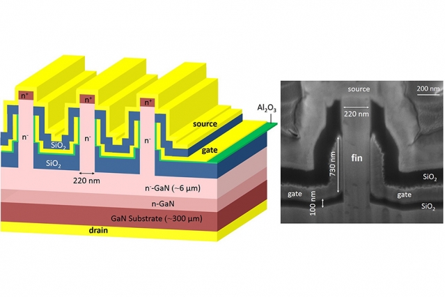
The thin and wide fins of these GaN transistors enable much higher-voltage operation and, subsequently, greater power handling compared to commercially available GaN transistors. Image source: MIT.
Developing higher-voltage vertical GaN transistors has been the focus of research for several years. Until recently, attempts to build vertical transistors with embedded physical barriers in the gallium-nitride semiconductor for the purpose of directing current into a channel beneath the gate haven’t met mass-production standards. This is likely due to the materials used to build these barriers being expensive and challenging to fabricate and could also involve long-term reliability.
Yuhao Zhang, a postdoc at MIT, and Min Sun, an MIT PhD graduate, participated in a different design strategy, one that may enable GaN transistors to reach several thousand volts. Diverting from the strategy of other researchers, Yuhao and Min fabricated narrower devices and a unique design strategy that dramatically increased the operating voltage without the use of exotic materials or techniques.
“Yuhao and Min’s brilliant idea, I think, was to say, ‘Instead of confining the current by having multiple materials in the same wafer, let’s confine it geometrically by removing the material from those regions where we don’t want the current to flow,’” said Palacios. “Instead of doing the complicated zigzag path for the current in conventional vertical transistors, let’s change the geometry of the transistor completely.”
Though they’re still unsure when, or if, this new technology will be commercially available, the researchers have at least demonstrated a viable method of producing much higher-voltage GaN transistors. This could lead to other research and commercial efforts to bring the efficiency and power benefits of GaN transistors to electrical grid, electrical vehicle, and renewable energy applications.
Advertisement
Learn more about Electronic Products Magazine


