Noise in chopper-stabilized amplifier applications
There are design tradeoffs on how to minimize noise in these circuits
BY WALTER BACHAROWSKI
National Semiconductor
Santa Clara, CA
http://www.national.com
A common complaint about chopper-stabilized amplifiers is that chopper noise will interfere with the signal and cancel the positive feature of almost-negligible offset voltage and offset-voltage drift. This is often claimed without fully evaluating the noise performance of the chopper amplifier in the application of interest. The amount of noise the amplifier will contribute depends on the closed-loop gain, and bandwidth as well as the value of the feedback resistors and the input referred voltage and current noise.

This article will show the output referred noise comparison of a low-noise nonchopper amplifier and a chopper amplifier under the same circuit topologies. Additionally, this will be primarily an empirical review that will display the effects of circuit changes on the noise performance without getting into depth on the math details.
By considering the required signal bandwidth, and closed-loop gain the noise performance of a chopper-stabilized amplifier can be as good as a non-chopper-stabilized gain stage while providing improved dc precision. Several design tradeoffs will be shown on how to minimize noise in chopper stabilized amplifier circuits.

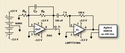
Fig. 1. The device-under-test (DUT) socket is set up so the gain resistors RF and RG can be easily changed along with the feedback capacitor CF .
Test setup
Figure 1 shows the experimental test setup. The device-under-test (DUT) socket is setup so the gain resistors RF and RG can be easily changed along with the feedback capacitor CF . The output of the amplifier being measured is ac coupled to amplifier A1 , which is a low-noise amplifier with a gain of 100 V/V. The noise voltage at the output of the device under test is equal to the noise voltage measured at the output of A1 divided by 100. This is the value used in the data tables.
The circuit is powered by a stack of four NiMH batteries which remove power supply noise from the measurement. The rms noise voltage is measured on an Agilent 34401A, 6.5-digit multimeter.
Test methodology
The goal of this article is to show the effects on amplifier output noise closed-loop gain, bandwidth, and input source impedance are varied and will provide some insight into the magnitude of these factors on the amplifier’s output noise.
The noise gain (NG ) of the amplifier being tested is NG = 1+ RF / RG , and it shows how much the noise sources at the input of the DUT are amplified. For this test RG will be 100 Ω or 1 kΩ, while RF will have the values 1k, 10k, and 100k, or 10k, 100k, and 1M, respectively. This provides three gains (11, 101, and 1,001) and two clusters of source resistances separated by a factor of 10. For each gain combination the value of CF has three values: 100 pF, 1,000 pF, or not installed.
The final variable is using the range of values with a chopper amplifier and nonchopper amplifier that have noise and bandwidth specifications that are relatively close. As an example, National offers a chopper amplifier such as the LMP2021 and a nonchopper amplifier, such as the LMP7701.
In this test setup, the noise of A1 is added to the noise from the DUT. One of the measurement corrections that must be evaluated is the noise floor of the measurement and includes the noise contributed to the measured noise value by A1 and the meter. To measure the noise floor the DUT socket is empty and J1 is connected to ground. The signal measured at pin 6 of A1 is the noise floor for the noise at the output of the DUT. The measured noise floor was 0.042 mV ac rms. The noise voltages add together as a square root of a sum of squares. The noise voltage measured by the meter that is contributed by the DUT is calculated as follows:
DUTNOISE = (√MeasuredNoise2 – NoiseFloor2 ) / 100

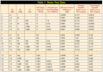
Table 1 shows the noise test data for both types of amplifiers.
Observations
The chopper amplifier has a wider bandwidth (5 MHz vs. 2.5 MHz) and a higher input referred noise voltage (11 nV/ vs. 9 nV/ ) than the nonchopper amplifier with the expected result of higher output noise at all of the data points. The noise contribution due to input noise current for both amplifiers is negligible at the source resistances being used.
The effect of reducing the source resistance can be see by the small reduction in noise voltages on a pair of comparable conditions, for example rows 1 and 2, 7 and 8, or 13 and 14.
The output noise can be reduced substantially by limiting the bandwidth of the amplifier. This can be seen in two ways. As the closed-loop gain increases the bandwidth decreases and the noise per unit of gain decreases. For example, comparing the noise voltage in rows 1, 7, and 13 for the chopper amplifier, the gain increases by 90 from row 1 to row 7, but the noise only increases by a factor of 5.7 while the gain increases by 900 from row 7 to row 13, but the noise only increases by a factor of 2.4. As the closed-loop gain of the amplifier increases the bandwidth decreases and limits the noise voltage.
The noise voltage can be significantly reduced by the use of a low-pass filter. CF in parallel with RF adds a pole to the feedback network which reduces the bandwidth and output noise. By comparing two rows of data in which only the level of filtering varies such as row 16 and 18, the significant reduction in noise voltage can be seen.
The closed-loop frequency response of an amplifier has a significant impact on the noise contribution to a signal path. By controlling the bandwidth and source impedances a chopper amplifier’s noise can be maintained at a low value while taking advantage of its almost zero offset voltage and offset voltage drift. ■
For more on chopper-stabilized amplifiers, visit http://www2.electronicproducts.com/AnalogMixICs.aspx.
Advertisement
Learn more about National Semiconductor


