NRZ-to-RZ data conversion using high-speed OR/AND
Fast Gbit/s gates provide straightforward solutions
BY BOB SCHWANKE and KEITH NELLIS
Inphi
Westlake Village, CA
http://www.inphi-corp.com
NRZ-to-RZ (non-return-to-zero to return-to-zero) data converters are critical components for ultra-long-haul transmission systems operating at data rates of 10 G and above. There are several ways to realize this function. We will describe one method that uses a general purpose OR logic gate.
NRZ and RZ communications
Due to its simplicity and low cost, NRZ is the standard signal format for optical communications. NRZ signals, however, are susceptible to impairments in the fiber, which limit how far the signals can be transmitted. For optical communications at 10 G and above, RZ transmission significantly increases transmit distance. Figure 1 illustrates the formats.
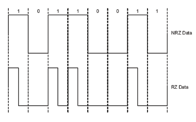
Fig. 1. Illustration of ideal NRZ and RZ signals.
RZ signals can be generated either in the optical or electrical domain. In the optical, an additional Mach-Zehnder modulator (the so-called “pulse-carver”) is used, which results in an expensive and bulky solution. In the electrical, a single, high-speed OR gate can be used, resulting in a very cost-effective, compact solution.
NAND and OR gate converters
An NRZ-to-RZ converter can be implemented simply by driving the inputs of an AND gate with NRZ data and a clock signal. Figure 2 shows a basic AND gate implementation and the appropriate timing for the input signals. The positive peak of the clock sinusoid needs to be centered within the data unit interval (data eye). This timing optimization ensures that the RZ output will not be distorted by an NRZ input data transition occurring while the clock is high.
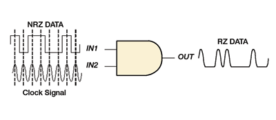
Fig. 2. Illustration of NRZ-to-RZ converter implemented with AND gate.
An AND function may also be implemented with an OR gate with its inputs and outputs inverted. Figure 3 illustrates the use of a differential OR gate as an NRZ-RZ converter. The width of the RZ phase pulses can be controlled by applying a dc threshold level to one of the inputs (VPW).
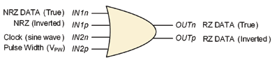
Fig. 3. Functional connections to differential OR gate.
Experimental results at 11.3 Gbits/s
The output signals for this experiment at 11.3 Gbits/s are shown in Fig. 4 using 13- and 25-Gbit/s OR gates. The clock input to each OR gate is properly centered within the input of the NRZ data eye as shown in Fig. 2.
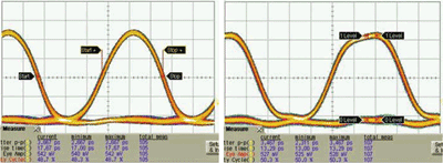
Fig. 4. 11.3-Gbit/s RZ signal output of 13-Gbit/s OR Gate (left) and 25-Gbit/s OR gate (right).
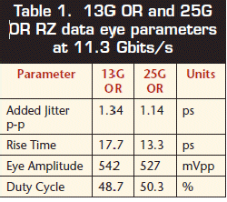
As Fig. 4 shows, the 13- and 25-Gbit OR gates produce high-quality RZ data outputs at 11.3 Gbits/s. Each gate reaches its full output amplitude, adds relatively low jitter to the input signal, and has a duty cycle that is close to 50%. The only noticeable difference between these two devices is that the 25-Gbit/s OR gate produces sharper edges and a more squared output.
If the system designer has bandwidth limitations elsewhere in the system the higher-speed 25 Gbit/s OR gate should be used to maximize signal quality and ensure overall bandwidth is not further degraded. Otherwise, the 13-Gbit/s OR gate will suffice. In general, it is recommended that the gate support data rates 20% higher than the RZ output data rate.
Experimental results at 25 Gbits/s
Figure 5 shows the RZ outputs of the 25- and 50-Gbit/s OR gates at a 25-Gbit/s data rate.
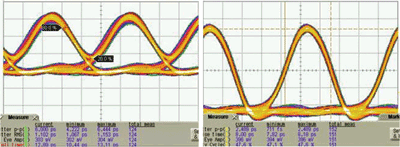
Fig. 5. 25-Gbit/s RZ output of 25 Gbit/s OR Gate (left) and 50 Gbit/s OR gate (right).
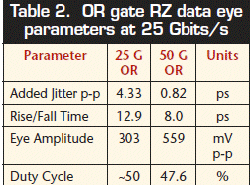
The RZ output eye of the 25-Gbit/s OR gate is distorted and has significantly reduced output amplitude (303 mVp-p) at 25 Gbits/s, compared to its typical output amplitude of 550 mVp-p. The 50-Gbit/s gate reaches its full output amplitude, so it is not band limited. The added jitter of the 50-Gbit/s OR gate is very low compared to the 25-Gbit/s device.
High-speed OR gates are available from a number of manufacturers. The devices used here are the 13612OR, 13613OR, 25712OR, 25713OR, 50712OR, and 50713OR 13-, 25-, and 50-Gbit/s chips from Inphi. ■
Advertisement
Learn more about Inphi


