Description
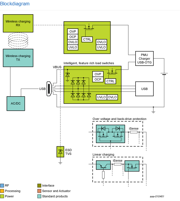
Whether a mobile device is charged via the USB port or a separate charger, it is exposed to incorrect polarity or abnormally high voltages. Any of these two occurrences poses a threat to the charger circuit and the PMU of the mobile device. In addition, the USB/charger port can be subject to ESD strikes and other transient discharges.
NXP offers an application specific portfolio of TVS diodes and ESD arrays, which enable cost efficient protection solutions – ESD, reverse polarity, overvoltage, other transient discharges – with the smallest footprint.
Li-Ion battery charging topologies
Battery chargers using external pass elements can be grouped into two main paths:
• Bipolar junction transistor (BJT) as pass element
o BJT as current regulator
o BJT as current regulator + MOSFET as control switch (Load switch)
• MOSFET as pass element with additional back drive protection such as:
o Single MOSFET + Schottky diode (FETky)
o Double MOSFET
NXP is offering cost efficient pass elements – bipolar transistors, MOSFET & FETky – for all use cases related to battery charging.
Often power management units (PMU) with an external pass transistor are capable of controlling a MOSFET, when used a switching element. As an alternative, a lower cost bipolar transistor, with very low VCEsat can be used instead. NXP’s low VCEsat (BISS) transistor performs the same function as a MOSFET at a lower cost, with no need for a reverse blocking diode. So a MOSFET + Schottky diode, or a double MOSFET, can be replaced by a low VCEsat (BISS) transistor and a resistor.
Download Full Block Diagram Below
Advertisement
Learn more about NXP Semiconductors


