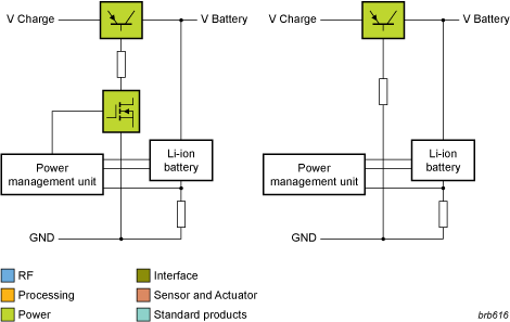
Description
Low VCEsat (BISS) transistor as pass element
Compared to voltage driven MOSFETs, BJTs are current driven devices. When designers want to replace a MOSFET with a BJT, they have to understand the current limitations of the PMU. To ensure the low VCEsat (BISS) transistor goes into saturation, the control pin of the PMU must be able to supply the base current (IB), otherwise an additional small-signal MOSFET control transistor is required. The control pin must provide 10 mA for the BISS transistor. BISS transistors can be used in saturation or linear mode. Both modes are shown in the diagrams above.
Key features and benefits
• High efficiency: Low VCEsat (BISS) transistors have lower forward resistance compared to similar rated MOSFET (latest devices enable ultra-low saturation voltage below 50 mV at 1 A)
• Low turn on voltage (typical VBE = 0.7 V compared to a MOSFET VGS = 1.8 – 10 V)
• Reverse blocking capability is an inherent function of BISS transistors, no additional blocking diode needed
• Positive gain vs. temperature coefficient
• High ESD level is an inherent function as opposed to non-ESD protected MOSFETs
• Current driven control loop is insensitive to supply voltage fluctuations
Download Full Block Diagram Below
Advertisement

Learn more about NXP Semiconductors


