OC, OV protection shrinks USB port electronics
Next-gen solutions, mini resettable fuses, and low-capacitance ESD suppressors protect USB interfaces
BY PAUL WIENER
Bourns, Riverside, CA
http://www.bourns.com
When the universal serial bus (USB) interface was introduced over a decade ago, its impact on consumer and industrial markets alike was grossly underestimated. Several standard revisions and billions of devices later, USB is as common to computing as the keyboard.
In order to deliver the convenience and speed available through USB 2.0, and the additional speed and power offered by the recently released USB 3.0 standard, designers must evaluate fundamental design-level considerations to ensure functionality and reliability of the hardware. As ICs continue to shrink in size and as data transfer rates increase, it is important to note that each time the interface is connected or disconnected, the port and its associated electronic components are subject to both overvoltage and overcurrent transients. Additional overvoltage and overcurrent threats include hot plugging, short circuiting, ESD events, faulty equipment, and user error.
To adequately manage USB port overcurrent and overvoltage protection needs, it is important to examine the use of next-generation protection solutions. Lead-free polymer positive temperature coefficient (PTC) devices protect circuits from potentially destructive overcurrent conditions.
Electrostatic discharge (ESD) suppressors and transient voltage suppression (TVS) products protect circuits from overvoltage, specifically ESD, electrical fast transient (EFT), and surge threats. As USB interface standards continue to evolve and change, combining these solutions can help protect sensitive USB ports, assist designers in speed of development and reduce total cost of ownership.
USB standards, concerns for protection
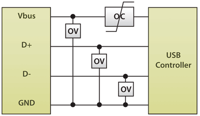
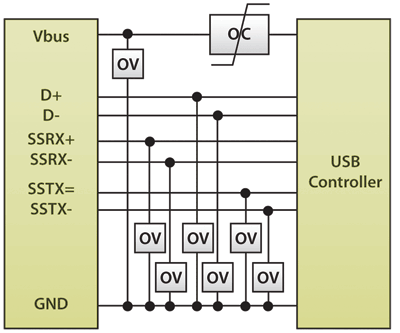
USB includes a four-wire interface with a pair of data lines, one power line operating at 4.4 to 5.25 Vdc, and ground through its 2.0 release. USB 3.0 adds a SuperSpeed differential data bus, achieves data transfer rates up to 5 Gbits/s, and specifies nearly twice the sourcing current of USB 2.0. USB 2.0 and 3.0 require the use of a resettable fuse for overcurrent protection on the power line. Every line requires overvoltage protection as illustrated below.

Fig.1. Protected interface through USB 2.0.

Fig.2. Protected USB 3.0 interface.
Overcurrent and overvoltage transients introduce separate protection concerns and thresholds for USB ports. USB 2.0 ports operate from tens of milliamperes to a maximal operating current of 500 mA, which is increased to 900 mA in USB 3.0. Overcurrent protection primarily focuses on resistance, which must be no greater than 700 mΩ with a maximal voltage drop of 350 mV, and reaction time. The fuse must react fast enough to prevent damage to the circuit and slow enough to prevent startup transients from tripping it (nuisance tripping). According to UL60950, a 5-A short must be removed in less than 60 s.
Overvoltage concerns focus largely on ESD protection based on the IEC Standard 61000-4-2 for the human body model (HBM), and are quantified by capacitance. The total USB interface line capacitance must be less than 10 pF with a signal clamping voltage under 6 V. By combining the technology and capability of next-generation resettable fuses and ESD suppressor devices, it is possible to choose the right options without sacrificing the integrity of the solution.
Resettable fuses for OC protection
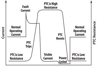
Resettable fuses exhibit a positive temperature coefficient (PTC) effect when heated, with the characteristic of exponential rather than linear increase in resistance with rising temperature. As the fuse temperature increases due to current or ambient temperature, the material expands, increasing the impedance from low to high by multiple orders of magnitude.
This transformation of the material allows the fuse to protect the load from overcurrent, within the rated limits of a device, creating a high-impedance circuit with slight leakage current. Once the current is removed, the material cools and returns to its highly conductive, low resistance state. The power must then be cycled in order to reset the device, generally resuming normal operation within one second. The entire process is illustrated in Fig. 3 .

Fig. 3. Current and resistance vs. time.
Next-generation designs
Manufacturers are introducing new technologies and manufacturing processes for superior performance and smaller sizes as the trend in miniaturization continues. One such technology, that we at Bourns call freeXpansion technology, limits the mechanical restrictions during the expansion of materials at the trip state and the contraction of materials upon reset.
This new technology allows for smaller surface-mount package sizes (0603/1608 metric), higher current- and voltage-handling capabilities, and improved resistance stability. These next-generation resettable fuses meet USB 2.0 and 3.0 voltage and current requirements, delivering reliable overcurrent and overtemperature protection with impedance as low as 3 mΩ.
ESD protection technology
ESD is the transfer of an electrical charge between two surfaces of unequal potential. ESD is the primary cause of IC malfunctions and can be extremely dangerous to sensitive electronic components. Four types of suppression technology are available to protect against ESD events:
• Polymer ESD suppressors use a printed circuit board (PCB) manufacturing process and polymer space discharge. The breakdown of the inserted polymer between the electrodes allows this device to work.
• Multilayer varistor (MLV) ESD suppressors use a thick-film manufacturing process and work through the breakdown of zinc oxide.
• The third technology uses an air gap design based on air discharge between two electrodes in a controlled air space.
Finally, TVS diode ESD suppressors use a thin film manufacturing process, operating through the breakdown of the p/n junction.
Next-generation ESD suppressors
Next-generation ESD suppressors are offered in a variety of package types and employ two basic technologies. One type uses polymer technology in surface-mount 1206 and 0603 packages providing a maximum capacitance of 0.5 pF for USB port protection.
This technology causes voltage charges to jump across the device in a stepping stone fashion. The distance between the metal particles within the component determines the ESD transient response of the device. Bidirectional protection is provided by the polymer-based device, and the repeatability is typically more than 100 hits.
The other option includes surface-mount 0603- and 0402-package sizes and employs a unique air gap discharge technology. This technology enables the device to distinctly control ESD and EFT.
Compared to the typical 5 pF of its TVS counterparts, the capacitance of some air gap devices is a mere 0.05 pF, leaving a full 9.95 pF for the designer to meet the 10pF maximal capacitance for the USB interface. The highest observed leakage current of 5 nA is far less than the 1 mA typical of most TVS components. Air gap discharge provides bidirectional protection and typically can withstand approximately 1,000 hits. Individual parts can be used or an array can protect four lines or more in a single package.
In discrete, array, and combo design packages, designers have the flexibility of incorporating these solutions into various different configurations. For additional information about Bourns circuit protection products including next-generation resettable fuses and ESD suppressors, visit http://www.bourns.com/ProductFamily.aspx?name=circuitprotection ■
Advertisement
Learn more about Bourns


