On-Demand Synaptic Electronics: Circuits that learn and forget
Researchers in Japan and the US propose a nanoionic device with a range of neuromorphic and electrical multifunctions that may allow the fabrication of on-demand configurable circuits, analog memories and digital–neural fused networks in one device architecture.
Synaptic devices that mimic the learning and memory processes in living organisms are attracting avid interest as an alternative to standard computing elements that may help extend Moore’s law beyond current physical limits. However so far artificial synaptic systems have been hampered by complex fabrication requirements and limitations in the learning and memory functions they mimic. Now Rui Yang, Kazuya Terabe and colleagues at the National Institute for Materials Science in Japan and the University of California, Los Angeles, in the US have developed two-, three-terminal WO3-x-based nanoionic devices capable of a broad range of neuromorphic and electrical functions.
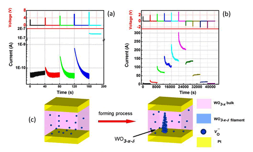
In its initial pristine condition the system has very high resistance values. Sweeping both negative and positive voltages across the system decreases this resistance nonlinearly, but it soon returns to its original state indicating a volatile state. Applying either positive or negative pulses at the top electrode introduces a soft-breakdown, after which sweeping both negative and positive voltages leads to non-volatile states that exhibit bipolar resistance and rectification for longer periods of time.
The researchers draw similarities between the device properties — volatile and non-volatile states and the current fading process following positive voltage pulses — with models for neural behaviour —that is, short- and long-term memory and forgetting processes. They explain the behaviour as the result of oxygen ions migrating within the device in response to the voltage sweeps. Accumulation of the oxygen ions at the electrode leads to Schottky-like potential barriers and the resulting changes in resistance and rectifying characteristics. The stable bipolar switching behaviour at the Pt/WO3-x interface is attributed to the formation of the electric conductive filament and oxygen absorbability of the Pt electrode.
As the researchers conclude, “These capabilities open a new avenue for circuits, analog memories, and artificially fused digital neural networks using on-demand programming by input pulse polarity, magnitude, and repetition history.”

(a): Volatile (short-term) memory property of two terminal Pt/WO3-x/Pt device before the forming process. Current change observed by applying sequence of positive voltage pulses at intervals of 40 s and widths of 0.5 s. Read voltage was 0.5 V. (b): Non-volatile (long-term) memory property in the device after forming process following application of sequence of positive and negative pulses with widths of 0.1 ms. Read voltage was 0.1 V. (c): Schematic illustration of the device structures before and after forming process.
Further Information
Publications and Affiliation:
Rui Yang1, Kazuya Terabe1, Guangqiang Liu1, Tohru Tsuruoka1, Tsuyoshi Hasegawa1, James K. Gimzewski1,2,3, and Masakazu Aono1, “On-demand nanodevice with electrical and neuromorphic multifunction realized by local ion migration”, ACS Nano, 6, 9515–9521(2012).
1.International Center for Materials Nanoarchitectonics (WPI-MANA), National Institute for Materials Science (NIMS), 1-1 Namiki, Tsukuba, Ibaraki 305-0044, Japan
2.Department of Chemistry and Biochemistry, University of California, Los Angeles, 607 Charles E. Young Drive East, Los Angeles, California 90095, United States
3.California NanoSystems Institute (CNSI), University of California, Los Angeles, 570 Westwood Plaza, Los Angeles, California 90095, United States
International Center for Materials Nanoarchitectonics(WPI-MANA)
Contact Information
1-1 Namiki, Tsukuba-shi Ibaraki, 305-0044 Japan
Email: TERABE.Kazuyanims.go.jp
Telephone: +81-29-860-4383
About Mana
http://www.nims.go.jp/mana/
Advertisement
Learn more about International Center for Materials Nanoarchitectonics


