ON Semi joins Imec’s GaN-on-Si research program
ON Semiconductor recently joined the multi-partner, industrial research-and-development program at Imec in order to participate on the development of next-generation gallium nitride (GaN) on silicon (Si) power devices. There has been a lot of talk about GaN since it is characterized by superior electron mobility, higher breakdown voltage, and good thermal conductivity properties, which make it ideal for power and RF devices that need high-switching efficiencies.
GaN-based power devices today are too pricey for large-quantity manufacturing, as they are fabricated on small diameter wafers using non-standard production processes. Imec’s broad-scale research program not only focuses on developing GaN-on-Si technology on 200-mm wafers, but it is also concerned of reducing the cost and improving the performance of GaN devices.

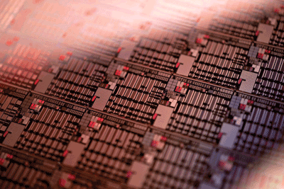
Imec’s power devices on 200- mm CMOS-compatible GaN-on-Si
By bringing together leading integrated device manufacturers (IDMs), foundries, compound semiconductor companies, equipment suppliers and substrate suppliers, Imec has been successful in achieving significant technical advancements.
This past year, Imec’s program successfully produced 200-mm GaN-on-Si wafers (as shown in image), bringing processing within reach for standard high-productivity 200-mm fabs. In addition, they developed a fabrication process compatible with standard CMOS processes and tools, the second prerequisite for cost-effective processing.
According to Hans Stork, senior vice president and chief technology officer at ON Semiconductor, “Partnering with imec will help strengthen our current market position and potentially assist us in adding a competitive leading-edge technology to our customer offerings. We look forward to collaborating with a broad consortium of like-minded companies on forward-looking research in this field.”
More information can be found on www.imec.be and www.onsemi.com.
Christina Nickolas
Advertisement
Learn more about Imec


