By Aalyia Shaukat, contributing writer
Two chemists at the University of Waterloo have discovered a method to control the orientation and size of single-walled carbon nanotubes (SWCNTs) — a major stumbling block in the mass production of carbon nanotube (CNT) transistors. While prior art relies on randomly growing nanotubes and establishing the best individual tubes to build a field-effect transistor with, this technique is the first that externally controls CNT parameters to tailor-make them for transistors.
The potential of carbon nanotubes
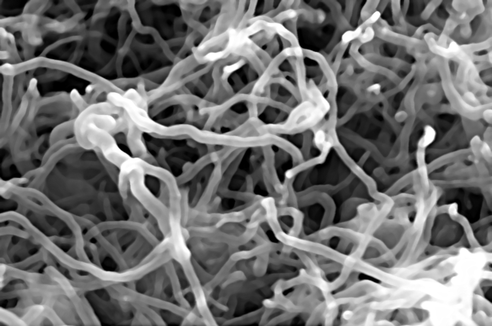
CNTs have been around for decades now as a potential replacement on the micro-level for silicon-based transistors and on the macro-level for copper interconnect. With the oft-cited Moore’s Law seemingly plateauing, alternatives for the robust silicon semiconductor technology are being researched such as diamond, germanium, and gallium nitride. Transistor performance heavily relies on two factors: the amount of current that flows through the channel and its energy efficiency. Traditional silicon-based MOSFETs have faced limits below the 22-nm range, particularly from the loss of current due to electron tunneling in the shorter channels. Furthermore, the thinner the channel, the simpler that it will be to turn the transistor switch on and off. SWCNTs are particularly unique as structure permits electrons to flow through it far faster than silicon, allowing for some pretty extraordinary field-effect mobilities. Additionally, the innately small size of CNTs (~1-nm diameter) allows for the gate to more easily control the flow of current along the length of the channel. Theoretically, CNTs are also able to conduct heat nearly as well as diamond or sapphire.
The obstacle
Unfortunately, the CNT’s bandgap is directly correlated to its diameter and chirality — a measurement structure’s asymmetry. A certain chirality will induce metallic properties in the SWCNT, and a metallic CNTFET would not be able to be switched off — a pretty undesirable outcome. Moreover, current methods to grow CNTs inevitably produce tubes with varying diameters and atomic topologies. CNTFETs were then generated by placing electrodes on top of hand-picked CNTs. While this process may be successful in developing individual transistors, it is not conducive to cheaply and reliably mass-produce integrated circuits (ICs).
A potential solution
The scientists at Waterloo have leveraged the Alignment Relay Technique to the control the orientation and size of CNTs. This method uses three-dimensional liquid crystals known as iptycenes to promote alignment as well as length and diameter selectivity.
“This is the first time chemists have been able to externally control the orientation of small molecules covalently bonded to a surface,” said Professor Schipper, a member of the Waterloo Institute for Nanotechnology. “We’re not the first ones to come up with potential solutions to work with carbon nanotubes. But this is the only one that tackles both orientation and purity challenges at the same time.”
Apparently, once setup, the process for controlling the purity (or percent of SWCNTs), dimensions, and orientation of the CNTs is relatively simple and can be done on a benchtop as opposed to a massive fabrication facility — a process that would have likely been eminently helpful in the creation of the world’s first CNT-based computer. While this is one small step toward realizing the concept of mass-producing CNT-based semiconductor technologies, it does eliminate some primary obstacles.
Advertisement
Learn more about Electronic Products Magazine


