The four basic building blocks of an op amp
BY TAMARA SCHMITZ
Senior Principal Applications Engineer
Intersil
www.intersil.com
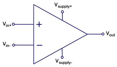
Operational amplifiers are the main building block of analog systems. They can provide gain, buffering, filtering, mixing and multiple mathematic functions. In system diagrams, they are represented by a triangle with five connections: positive supply, negative supply, positive input, negative input and output (see Fig. 1 ). The supply pins are used for powering the device. They might be connected to ±5 V, for example, or with special consideration, be connected to 10 V and ground. The relationship between the outputs and the inputs is straightforward:
VOUT = A (VIN+ VIN- )
Which means that the output voltage is equal to the gain (A) of the amplifier times the difference of the input voltages.

Fig. 1: The common input and output pins of an op amp.
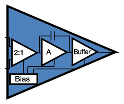
Many engineers never need to know what happens inside this magical triangle. Have you ever been curious? There are four basic sections: bias, 2:1, gain and buffer (see Fig. 2 ). These four stages can be combined in some op-amp devices, but the four functions are fundamental.

Fig. 2: The four internal blocks of an op amp.
Bias section
The bias section provides all of the voltages and currents needed by the other three sections. When you dive into this section, you find circuits like bandgaps and current mirrors. Bandgaps are small circuits that provide a constant voltage. Although that may seem like an easy task, the voltage must be constant even if the supply voltage changes or if the temperature changes. These effects can be larger than you expect, so they must be planned for and canceled out.
Current mirrors take a given current and create copies of it for other circuits. By scaling the size of the transistors or placing multiple mirrors in parallel, these currents can be properly sized as well. This powerful technique allows the op-amp designer to scale the amount of current into each stage. The bias section often consumes a very small fraction of the total current while the buffer stage consumes the most on-demand current to drive an output load.
2:1 section
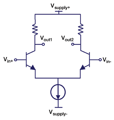
Given that an op amp has two inputs and one output, there has to be a 2:1 stage somewhere inside. This may be very close to the input or later in the signal path. In the simplest form, the circuit that performs this action is called a differential pair. A differential pair is two transistors hooked to a common current source, as in Fig. 3 . The operation of this circuit is much like a seesaw. On a seesaw, either side can adjust the balance. If I’m on one side and you are on the other, I can raise—which causes your side to lower. If instead I drop my side, then your side raises. If we correlate height of each side of the seesaw with the amount of current that flows through each side of the differential pair, you’ve got it! In this way, the non-inverting input controls one side of the circuit and the inverting input controls the other side of the circuit. Whichever side has a larger input voltage will have larger current.
Let’s think about what happens when both sides have the same voltage. Remember the seesaw. If you and I exert the same amount of pressure (weight) on both sides of the seesaw, who’s side will be higher? Neither! They will be the same height. What happens if we both apply more pressure? If we both apply the same amount of pressure, then the seesaw stays balanced. The only way the seesaw will move is if one of us applies more pressure than the other. Another way of looking at this is to say that the seesaw will only respond to differences in pressure. That is exactly the way the inputs of the differential pair (and the inputs of the op amp) work.

Fig. 3: A simple 2:1 stage.
Achieving the 2:1 function is easier than you might expect. In the differential circuit shown in Fig. 3 , there are two inputs and two outputs. A 2:1 circuit would only have one output. Okay, then let’s ignore one of the outputs. That may seem crude, but it’s been done many times. There are extra transistors you can add to the unused side if you want to fold and sum the currents back together, but they aren’t necessary. It all depends on what you are optimizing for. For example if you are optimizing for space or simplicity, then there is no need for the extra circuitry.
The critical parameter of this section is offset voltage. Back to the seesaw, what if I installed a comfortable chair on my side? You would have to add pressure/weight to your side (without the chair) just to balance the seesaw. The same can occur with the transistors. Offset appears if the two transistors composing the differential pair aren’t exactly the same size or shape. Designers do their best to create exactly duplicate transistors, but their efforts can be limited by available space or even the structure of the equipment used to fabricate the integrated circuit.
Gain section
Gain means the output is bigger than the input. To use a basic financial analogy, if your investments gain, you have more money. If your investments go down, you lose money. Since an op amp’s primary role is to provide gain, this is the flagship section of the device. In an ideal op amp, the gain is infinite. That means that the smallest difference in the input voltages causes the output to slam up or slam down. Luckily, the power supplies limit how far the output can travel, so the output doesn’t have to reach thousands or millions of volts in the positive or negative direction. In the simplest form, the gain function can be provided by a single transistor. If a single transistor can provide gain, why do we need to collect many of them to create an op amp? A single transistor has one input and one output. The op amp needs two balanced inputs and more gain than a single transistor can provide.
Since this section has the largest amount of gain, it is also the section where we would include compensation. Compensation in an op amp means creating stability. Let me offer a bit of intuition:
With lots of gain, a small input signal will cause a very large output signal. Similarly, if the input voltage changes from zero to small, the output would have to change from zero to large. The larger the gain or the faster the input changes, the faster we need the output to respond. Fast circuits need more control. Think about all the feedback and support that goes into driving a race car at 200 mph. There’s an entire pit crew needed. Now think about what is needed to drive a golf cart. It’s much easier and takes much less skill to drive a golf cart. Going back to the circuit from this analogy, the race car would need a lot of compensation to keep it stable (keep it from crashing) while the golf cart would need very little, if any compensation. Compensation in op amps takes the form of a capacitance, shown in Fig. 2 connected between the input and output of the gain stage.
Buffer stage
The buffer stage serves two critical functions. First, it protects the gain circuit from anything that can be connected to the output. Secondly, it drives the load. That means it can provide the current needed to take the load to the correct output voltage. This stage provides no gain, which means that the input voltage and the output voltage are the same size. Instead, it provides more current, which translates into more power. Think of it like training in the U.S. Army. A colonel could go and fight with all of his skills, but if he teaches those skills to an entire battalion, the force of the group is far stronger. This is very similar to the action of a buffer. The output tracks the input to the best of its ability with the force of a larger current, making it Army strong.
When examining output stages, you will find different classes: A, AB, B, C, and more down the alphabet. Class A is the simplest stage with the most linearity, but also burns the most power. Class B and C are related, each slicing away different parts of the output signal to adjust for offsets needed to turn on transistors. There are many other output stage circuits. Some include transformers, some use transmission lines and some use clocked signals. All have been optimized for specific applications. A plethora of information is available if you want to learn more.
Bringing it all together
So we can define an op amp as a seesaw on a race car followed by an Army battalion fueled by the nourishment of the bias section. (I wouldn’t suggest putting that on a T-shirt or sharing this with one of your company’s technical fellows.) It is a unique device that provides so many wonderful functions. The balanced input creates the perfect opportunity to allow for feedback. Feedback will allow us to control gain, to trade it for bandwidth and performance and to stabilize systems.
For now, let us celebrate the four main blocks that make the op amp a pillar of the analog community. Whether you use five transistors or 500, an appreciation and understanding of those internal circuits empowers you to find new ways to use the greatest analog building block, the op amp. To find a useful parametric search tool for different kind of op amps, go to www.intersil.com/amps/. ■
Advertisement
Learn more about Intersil


