Key parameters that must be considered when selecting an amplifier for this type of application
BY KEVIN TRETTER
Microchip Technology
Chandler, AZ
http://www.microchip.com
Medical applications continue to drive new innovations within the semiconductor field. From glucose meters that last longer to implantable pace makers that are even safer, semiconductors play a critical role in turning these concepts into reality.
Advances in integrated circuits used in medical imaging have made this technology more useful and affordable. As a direct result of these advancements, the use of computed tomography (CT) scans has increased 20-fold over the past 30 years.
CT scanner
A CT scanner can produce three-dimensional images of an object based upon a large collection of two-dimensional X-rays. A critical component of this system is the circuitry that detects the X-ray signals.
As the X-rays pass through the object being examined and into the scintillator, the visible light generated by the scintillator will fluctuate, causing the output of the array of photodiodes to fluctuate in terms of the resulting current flow.
A large collection of these two-dimensional X-rays are then combined with sophisticated computing software to produce both two and three-dimensional images. This technique can create amazingly accurate images, and can even capture the beating of a human heart!
Front-end detection circuitry
As mentioned above, an array of photodiodes produces an electrical current based on the detected light. This low-level current must be properly conditioned so that the information can be correctly converted to a digital signal for further computation.
A key element of this signal-conditioning circuitry is the amplifier. An amplifier is used to convert the electrical current to a voltage, to provide gain and filtering, and to buffer the signal prior to its being converted to a digital signal via an A/D converter. Several key parameters must be considered when selecting an amplifier for this type of application.
Input offset voltage
The current produced by a photodiode is relatively small in magnitude, and any change in current must be accurately captured in order to reproduce the proper image. In addition to converting this low-level current to a voltage, an amplifier can also provide gain, increasing the resolution of the detector circuitry.
For such applications, the amplifier’s offset voltage becomes critical. As the name implies, this specification is the amplifier’s voltage difference between the inverting and non-inverting inputs. This voltage offset depends on the amplifier’s topology, and can range from microvolts to millivolts in magnitude.
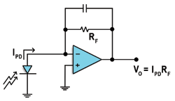
Fig. 1. A simple transimpedance amplifier configuration which uses a photodiode acting as a current source.
Figure 1 shows a simple transimpedance amplifier configuration with a photodiode acting as a current source. In this example, the current generated by the photodiode, IPD, is multiplied by the resistor, RF, to create a voltage on the output of the amplifier, VO. For example, let’s assume RF is 100 kΩ. A 10-μA change in the photodiode current would create a 1-V change on the output.
However, the amplifier’s input offset error will add directly to this output voltage. If the amplifier in the above example has an input offset voltage of 5 mV, then the output of the amplifier would be 1.005 V instead of 1 V, resulting in an error of 0.5%.
Input offset voltage drift
Like all electrical components, amplifiers change behavior over time and temperature. This is certainly true of the amplifier’s voltage offset. As noted above, the voltage offset is a source of error. As the offset drifts, this error could become even greater. This error source can be minimized by selecting a low-drift amplifier, such as an amplifier with an auto-zero based topology, or implementing periodic system calibrations to calibrate out the offset and drift.
As an example, Microchip Technology recently introduced a family of amplifiers that feature mCal technology (see Fig. 2 ), which is yet another way to combat the adverse effects of voltage offset and offset drift. The mCal technology is an on-chip calibration circuit that corrects the offset-voltage error of the amplifier. This calibration circuitry is active upon power-up or based on the state of a calibration hardware pin. The calibration pin allows the user to initiate a calibration routine at any time, thereby minimizing the effects of offset drift.
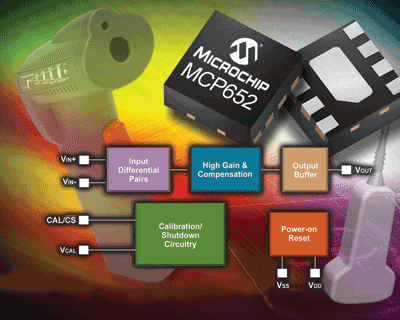
Fig. 2. New developments in op-amp design includes on-chip calibration circuitry.
Input bias current
Another source of dc error in a transimpedance application is due to the amplifier’s bias current, the amount of current flow into the inputs of an amplifier to bias the input transistors. This current can be thought of as a leakage current, but is referred to as a bias current when on the inputs of an amplifier.
This bias current can range from picoamperes to hundreds of nanoamperes. Amplifiers with a CMOS input stage generally have less bias current, when compared to an amplifier with bipolar input transistors.
Just like the current generated from the photodiode, as shown in Fig. 1, the bias current of the amplifier will be multiplied by RF and create an error voltage at the output of the amplifier. In the above example, an input bias current of 100 nA, which isn’t unreasonable for a bipolar amplifier, will create a 1-mV error on the output, or 0.1%. By selecting an amplifier with a CMOS input stage — and therefore low-bias currents — such as the MCP652, this error source can be minimized.
Bandwidth/frequency response
As the visible light generated from the X-ray tube passes through and around an object, it fluctuates, thereby causing the output of the array of photodiodes to fluctuate in terms of the resulting current flow. These fluctuations must be accurately captured by the amplifier and the rest of the signal-conditioning circuitry. Therefore the amplifier’s usable bandwidth and frequency response are important. If the system is too slow, information can be lost or misrepresented prior to digitization.
Amplifier output swing
In the example used previously, a 10-µA current from the photodiode produced a voltage change of 1 V on the amplifier’s output. For a 5-V single-supply system, this would suggest that the amplifier circuitry could accurately detect currents from zero to 50 µV, assuming the amplifier output could swing to both supply rails. If the amplifier did not support rail-to-rail output swing, the overall range of current that could be accurately detected would be less, hence limiting the dynamic range of the detection circuitry.
Amplifier noise
Another important parameter that must be considered when evaluating amplifiers for this type of application is the amplifier noise. Keep in mind that an amplifier’s noise may not be constant over frequency, especially at low frequencies where 1/f noise can become the dominant noise source. This low-frequency noise is critical when the input signal is near dc.
As the world of medical imaging continues to advance, system designers continue to be faced with new challenges. Likewise, semiconductor manufacturers must continue to find innovative solutions. For the example mentioned, mCal not only provides a means of obtaining a low initial input offset voltage, but also a way to combat the adverse effects of drift over time and temperature. These are critical specifications in high-precision instrumentation applications, including front-end detection circuitry for CT scanners. ■
Advertisement
Learn more about Microchip Technology


