By Chris Glaser, senior applications engineer, Member Group Technical Staff, Texas Instruments, www.ti.com
Many systems operating from a small-capacity battery require a high-efficiency switching DC/DC converter to lengthen the operating lifetime between battery recharges. However, many of these systems also require the low noise of a low-dropout linear regulator (LDO) to power sensitive analog circuits such as sensors, radios, or data converters. Extremely limited printed circuit board (PCB) space further complicates the power-supply design for smartwatches, fitness trackers, earbuds, and other consumer and medical wearable devices.
The trade-offs of efficiency, output noise, and size require optimized solutions for each specific system. This article compares the three fundamental power architectures of DC/DC-only, LDO-only, and DC/DC followed by an LDO, keeping in mind their suitability for specific applications.
System architecture
Numerous portable devices operate from a single-cell rechargeable lithium battery, with a voltage range of about 3 V to 4.2 V. Many disposable medical devices operate from primary (non-rechargeable) chemistry batteries, such as coin cells and AA or AAA alkaline. In many cases, the power supply must also operate from a USB port, which provides voltages of 5 V and above. The power supply takes this input voltage and lowers it down to the various voltages required by the system loads, such as 1.2 V. Either a step-down (buck) DC/DC converter or an LDO reduces the voltage.
A typical DC/DC converter is more efficient than a typical LDO, but the DC/DC has higher noise than the LDO. The two converters are often combined, with the LDO placed after the DC/DC, to reduce output noise while still maintaining good efficiency. However, this requires a larger PCB space and the higher cost of two devices.
Fig. 1 shows an example of the DC/DC-plus-LDO architecture. The DC/DC steps down the input voltage to 1.4 V, while the LDO reduces the 1.4 V to the 1.2 V required by the load. The LDO’s BIAS pin allows a very low 200-mV dropout voltage, which increases the overall efficiency while still providing good noise rejection.

Fig: 1: Block diagram of the DC/DC-plus-LDO architecture.
Alternatively, you could remove the LDO and the DC/DC could output 1.2 V directly. This is the DC/DC-only circuit. Or you could remove the DC/DC from Fig. 1 and have the LDO drop the input voltage to 1.2 V directly. This is the LDO-only circuit. These three configurations have various advantages and disadvantages.1
Efficiency
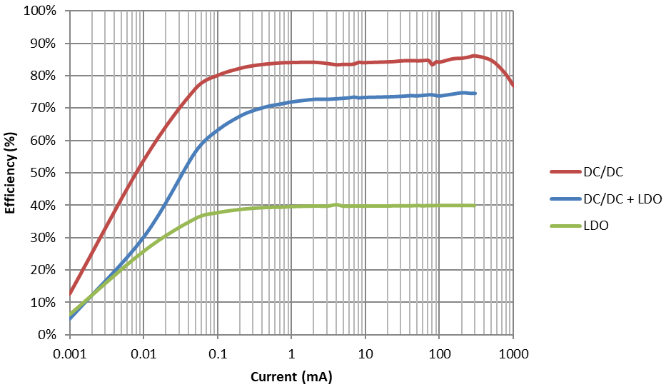
A power supply’s efficiency determines how long a battery lasts before needing to be recharged or replaced. Because this run time is a critical feature in most portable systems, the highest-possible efficiency is desired. This favors a DC/DC-only architecture; however, the output noise from some DC/DCs is too high for some loads. In these cases, adding an LDO after the DC/DC provides higher efficiency than an LDO-only architecture and slightly lower efficiency than the DC/DC-only architecture. A DC/DC-plus-LDO architecture is preferable for high-performance systems in which the load requires the lowest noise. Fig. 2 compares the efficiency of the three architectures with a 3-V input voltage and a 1.2-V output voltage.

Fig. 2: Efficiency comparison of the three power architectures.
The Texas Instruments (TI) TPS7A10 LDO is designed to follow a DC/DC to create low output voltages and is limited to input voltages below 3.3 V. If you need to support higher input voltages with an LDO-only architecture, TI’s TPS7A05 is a low-quiescent-current (IQ ) choice that supports up to 5.5 V.2 As the input voltage increases, the efficiency of the DC/DC-only and DC/DC-plus-LDO architectures decrease slightly. The LDO-only architecture’s efficiency decreases linearly with the input voltage, as the efficiency of any LDO is approximated by

Because of this, the LDO-only architecture is popular when the difference between the input voltage and output voltage is low. For example, dropping a 3.6-V battery voltage to a 3-V output voltage with an LDO is 83% efficient.
At very light loads, below about 10 µA, the power supply’s IQ dominates efficiency. The TPS7A10 LDO boasts an IQ of about 6 µA, while the TPS62801 DC/DC offers just 2.3 µA of IQ . An even lower IQ — and a corresponding higher efficiency at very light loads — is possible with devices such as the TPS7A05 LDO (1-µA IQ ) and TPS62743 DC/DC (0.360-µA IQ ). Alternatively, higher efficiency at higher loads is possible through the reduced switching frequency in the TPS62807. Through device selection, one parameter (for example, efficiency) is maximized while trading off other parameters, such as size, cost, and maximum output current.
Output noise
There are numerous ways to measure the output noise of any power supply, so I will give only two examples: measuring the output ripple with an oscilloscope in the time domain and measuring the output noise density with a spectrum analyzer in the frequency domain.
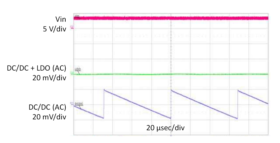
Fig. 3 shows the DC/DC-plus-LDO architecture’s output ripple measurement at a 3.6-V input voltage and 1-mA load current. The DC/DC operates in power-save mode to achieve the highest efficiency but has a low operating frequency and a higher ripple.3
The lower frequency is easily rejected by the LDO’s power-supply rejection ratio (PSRR) to remove any trace of ripple. Having a low-enough ripple at a high-enough frequency is critical for powering radios, such as Bluetooth Low Energy, without affecting their sensitivity.

Fig. 3: Output voltage ripple of the DC/DC-plus-LDO architecture.
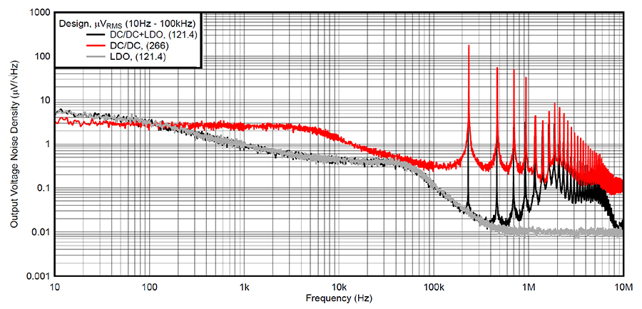
Fig. 4 shows the measured output voltage noise density of all three power architectures at a 3-V input voltage and 10-mA load current. The output noise is integrated over a frequency band (generally 10 Hz to 100 kHz) and then summed to produce a total root-mean-squared (RMS) noise value in microvolt RMS (µVRMS ) units. As expected, the LDO has the lowest total noise even when it is used after the DC/DC. The peaks in the DC/DC and DC/DC-plus-LDO curves represent the DC/DC’s switching frequency and its harmonics. The LDO clearly reduces the amplitude of this switching noise.

Fig. 4: Output noise density comparison of the three power architectures.
Solution size
For any switching DC/DC converter, the switching frequency is inversely proportional to the solution size and the efficiency. A higher switching frequency allows a smaller and lower-height inductor and capacitors while reducing efficiency due to increased switching losses. Modern DC/DC converters designed for small portable applications use innovative techniques to achieve a very small size and high efficiency.
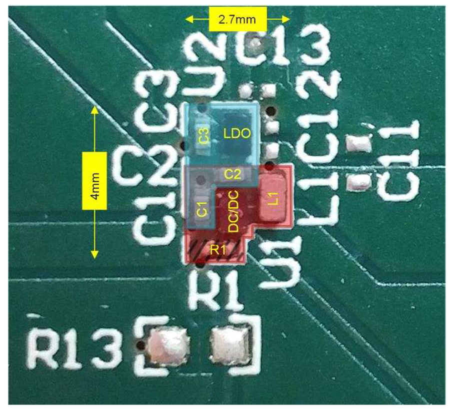
Implementing a 4-MHz switching frequency and wafer chip-scale packages (WCSPs), the TPS62801 DC/DC and TPS7A10 LDO combine for a tiny total solution size of 8.5 mm2 . The pinout of each device and the PCB layout are optimized in such a way as to share capacitors (C1 and C2 in Fig. 5 ) between both devices. The high DC/DC switching frequency enables operation with the smallest passive components: 0201 (0603) capacitors and a 0402 (1005) chip inductor. Fig. 5 is a zoom-in of the actual PCB layout, which uses 250-µm component-to-component spacing.

Fig. 5: Actual solution size of the DC/DC-plus-LDO architecture.
The DC/DC-only architecture’s components occupy just 5.5 mm2 , while the LDO-only architecture would occupy about 4 mm2 . While all wearable applications need a small solution size, some applications need the smallest possible size. Many medical sensor patches (and other in-body applications, for example) require both the lowest output noise and smallest size of an LDO-only architecture. Adding a DC/DC to increase the efficiency simply doesn’t fit.
Conclusion
Designing a small, battery-powered system requires trade-offs between efficiency, output noise, and size. Smartwatches and fitness trackers, which are slightly larger than earbuds or medical patches, use power architectures with DC/DCs for the highest efficiency. But even those systems have certain rails, such as for sensors and data converters, that require the lowest-noise LDOs. Table 1 summarizes the trade-offs discussed in this article, based on the example design in Reference 1.

Table 1: Efficiency, output noise, and size comparison of the three architectures.
Within the broad categories of DC/DC and LDO, Texas Instruments offers a variety of devices to optimize these three key priorities for different applications. Even with the variety of systems in the world, there is likely to be a power-supply architecture suitable for every design.
References
1. Light Load Efficient, Low Noise Power Supply Reference Design for Wearables and IoT.
2. Glaser, Chris. “ IQ : What it is, what it isn’t, and how to use it .” Texas Instruments Analog Design Journal, 2Q 2011.
3. Glaser, Chris. “ High-efficiency, low-ripple DCS-Control™ offers seamless PWM/power-save transitions.” Texas Instruments Analog Design Journal, 3Q 2013.
Advertisement
Learn more about Electronic Products MagazineTexas Instruments


