Advances in IC technology have led to enhancements in both ovenized (oven-controlled) crystal oscillators (OCXOs) and temperature-compensated, voltage-controlled crystal oscillators (TCVCXOs) that have blurred their historical differences. As technology has improved, the functionality of both types of oscillators has made it difficult for many designers to determine which technology is appropriate for a particular application. TCVCXO technology has been developed to a point where it is a viable option in applications where only OCXOs were an option.
This article provides the designer with information pertaining to the enhanced performance characteristics of current TCVCXO technology and briefly compares that performance to OCXO technology. The data presented here is taken from commercially available, off-the-shelf OCXOs and small-cell-grade TCVCXOs. Exact numbers will differ between manufacturers, but the general trends and approximate magnitudes should be similar.
TCVCXO technology
A TCVCXO is a voltage controlled crystal oscillator with a correction voltage applied to the voltage control pin. This correction, or compensation, voltage changes with temperature to bring the frequency back to nominal. This application exercises the crystal over the entire frequency range of the specification. However, any crystal-related issues (such as coupled modes), cannot be corrected and are superimposed on the resulting frequency-temperature curve; this makes the design and manufacturing of the crystal a difficult and critical part of the TCVCXO.
The majority of TCVCXOs require a voltage-control function to allow for exact setting of frequency, adjustments for long-term aging, and the ability to phase lock the device to other sources. This TCVCXO function works by adjusting the load capacitance presented to the crystal. Most small-cell requirements include a voltage-control option.
Exact TCVCXO specifications vary with the manufacturer. In general, small cells require ±0.1 ppm stability over a specified temperature range: one of the more common specifications is 0 to 80°C with ± 5 ppm of pullability for the voltage-control function. It is only in the last several years that crystal technology has improved to the point where crystals could be reliably compensated to this level. There are a number of technical issues to consider in the manufacture of these crystals. The crystals for the TCVCXO must be produced free of perturbations, with very low aging characteristics as well as extremely low hysteresis characteristics.
The frequency-temperature and hysteresis characteristic for today’s small cell grade TCVCXO (fig. 1 ) provides a performance level that would have typically been delegated to the OCXO realm not long ago. Improved semiconductors and optimized crystal design and manufacturing processes make it possible for TCVCXOs to compete in the ±0.1 ppm stability realm. The correction voltage required to adjust frequency for drift and long-term aging characteristics is usually generated by NTP, PTP (IEEE-1588) implementation. TCVCXOs have very low aging rates and very linear characteristics with regard to the control-voltage function.
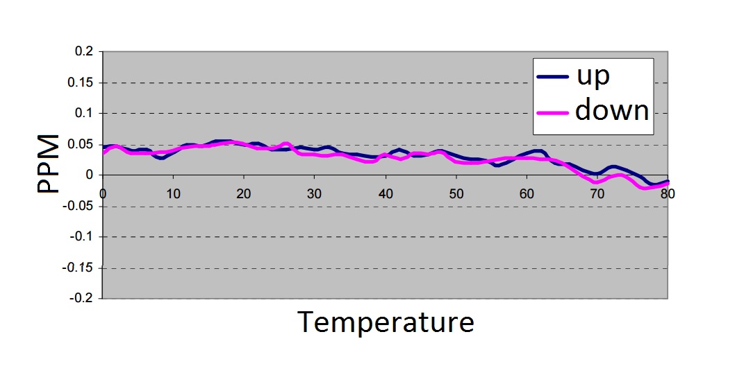
Fig. 1: The frequency-temperature and hysteresis characteristic shown here for today’s small-cell-grade TCVCXO, would have only been possible with an OCXO in the past.
Not only do precise compensation, low hysteresis, and low aging rates make TCVCXOs an exceptional solution for small cell applications, but they also provide low power consumption. For this application, TCVCXOs use approximately 2 mA, whereas an OCXO would require approximately 100 mA. Their size, power requirements and warm-up time place traditional OCXOs at a significant disadvantage when compared to TCVCXOs designed for this application.
OCXO technology
Ovenized crystal oscillators are typically used for high precision frequency control applications. This approach heats the crystal and associated oscillator circuitry to the upper turning point of the crystal (fig. 2 ).
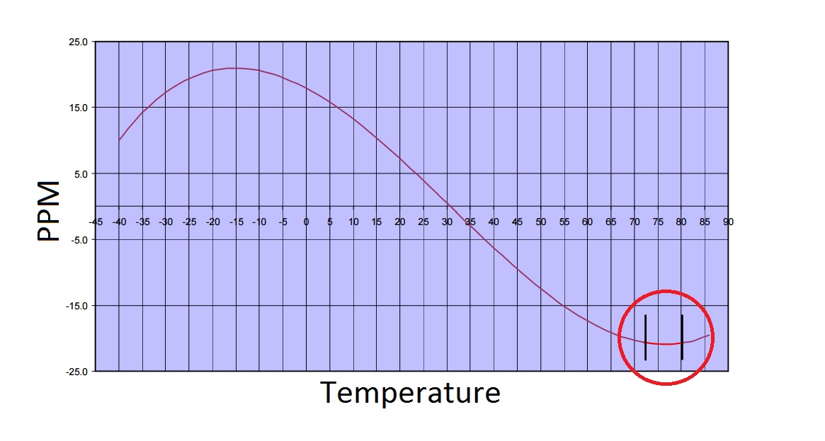
Fig. 2: The upper turning point of the OCXO shown here is used in the OCXO application.
The crystals for these oscillators are manufactured so the upper turning point is above the highest specified temperature range. The crystal and associated circuitry is heated to and maintains a narrow temperature window around that point on the crystal, and the device is tuned to frequency at that temperature.
The OCXO has an advantage in only exercising the crystal over a very narrow temperature window, typically a couple degrees or less. This greatly reduces the chances of exciting unwanted modes in the crystal. By contrast, a TCVCXO electrically compensates for the crystal characteristic. This places a strong emphasis on the quality of the crystals being used in these applications.
Table 1 outlines the differences between OCXO and TCVCXO products. In general, TCVCXOs are preferred when size and power are critical to the application. OCXOs historically had an advantage with a lower sensitivity to small stability changes when changing the voltage-control functions to the max or min value. However, the semiconductors used for small-cell-grade applications have compensation circuitry for that function; the improved performance makes TCVCXOs extremely competitive with OCXO technologies.
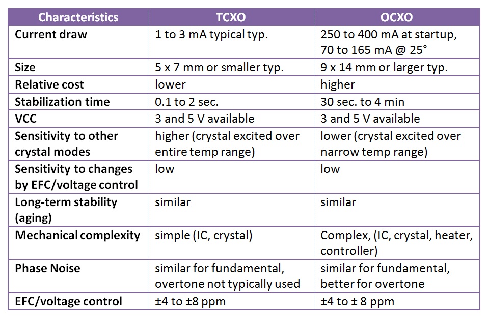
Table 1. Comparison of OCXO and TCVCXO characteristics for small cell applications
Advertisement
Learn more about Pletronics


