BY ROGER H. GRACE
President, Roger Grace Associates
www.rgrace.com
While there are a number of printed/flexible (P/F) sensors available today [1] , leading research universities and institutes worldwide are engaged in even more interesting, advanced developments.
Among those research centers, and this is not an exhaustive list, are Imec Holst Centre, Northeastern University’s Center for High-rate Nanomanufacturing, University of California at San Diego’s Jacobs School of Engineering Center for Wearable Sensors, the F. Seitz Materials Research Laboratory at the University of Illinois at Urbana-Champaign, VTT Technical Research Centre Ltd in Espoo, Finland, Center for Personalized Health Monitoring at the University of Massachusetts, Amherst, and, in Germany, Fraunhofer EMFT, Munich, Fraunhofer ENAS, Chemnitz, and Fraunhofer IZM, Berlin. Examples of the work of these researchers is given here; unfortunately, space and time do not permit discussion of the work being done at Arizona State University, Clemson University, Stanford University, UC Berkeley, and Western Michigan University.
Advanced developments
The Imec Holst Centre has developed several P/F sensors, including a solid-state, ion-selective electrode for monitoring pH, Cl, Na and K. Additionally, they are developing sensor labels built on ultra-thin (less than 150 µm) polyester foils that can measure humidity, temperature, chemicals, and gases and include NFC/RFID functionality.
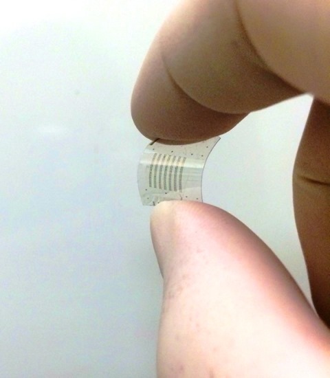
Northeastern’s Center for High-rate Nanomanufacturing (CHN) has developed a simple and highly sensitive multi-biosensor containing semiconductor single-walled carbon nanotubes (SWCNTs) that are enzyme-immobilized for detecting D-glucose, L-lactate, and urea in sweat (fig. 1 ). CHN’s director, Prof. Ahmed Busnaina, notes that, “The utilization of semiconducting carbon nanotubes for electric detection results in high repeatability and sensitivity. By leveraging the advantage of the carbon nanotubes’ electrical response and enzyme reaction, fast, specific, and continuous detection is achieved. Printing of nanomaterials to create the sensor results in low manufacturing cost”. [2]

Fig. 1: Researchers at Northeastern University’s CHN have created a flexible biosensor, based on single-walled carbon nanotubes (SWCNTs), for real-time pathogen detection and physiological monitoring. Semiconducting SWCNTs are functionalized with specific molecules for detecting pathogens, glucose, lactate, urea, and such, and printed on a flexible substrate.
UCSD’s Center for Wearable Sensors is also developing biomedical sensors. Prof. Joe Wang of the Center explains that “Our team has developed a skin-worn tattoo-based wearable electrochemical device which includes electrolyte and metabolite sensors, a biofuel cell, and batteries [fig. 2 ]. Temporary tattoos are attractive platforms for fabricating skin-worn devices. Body-compliant wearable electrochemical devices on temporary tattoos couple highly favorable substrate-skin elasticity with attractive electrochemical performance.” [3]

Fig. 2: Researchers at the University of California, San Diego, (UCSD) Center for Wearable Sensors have developed a printed/flexible/stretchable “tattoo” of electrochemical sensors that can be applied to a subject’s arm to monitor analytes — chemical constituent of interest in an analytical procedure.
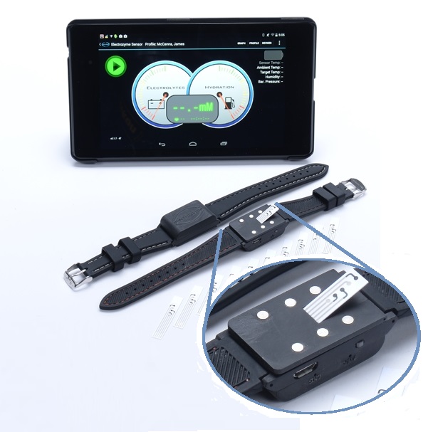
A few of Prof. Wang’s students formed Electrozyme (www.electrozyme.com) to commercialize this work. They have developed and licensed a flexible epidermal bio sensor system that can be used to determine the dehydration level of the wearer. The sensor suite consists of their P/F electrochemical sweat sensing device on a 7 x 40-mm PET substrate, along with several other externally sourced non-P/F sensors (which may include temperature and humidity at a minimum), and with some application algorithms provided by their “partner” customer. During intense exercise or other physical activities, the system will assist users in determining the quantity, intensity, and chemical composition of the fluids that the user will need to ingest to overcome the problems associated with de-hydration. Working with their integrator partner, this product (fig. 3 ) is expected to reach the market in the second or third quarter of 2016, according to Electrozyme CEO Josh Windmiller.

Fig. 3: Using intellectual property licensed from UCSD to create a wrist-wearable hydration sensor that will soon to be introduced by its development partner, Electrozyme uses its electrochemical chemical printed/flexible sensor with other, outsourced sensors to inform the wearer of what, when, and how much they should ingest to prevent dehydration.
Another spin-out working on biomedical P/F technology, this time from Professor John Rogers' materials science laboratory at the University of Illinois, is Cambridge, MA-based MC10 Inc. The MC10 team has been developing a new class of soft, conformal electronics and sensors that laminate on the human skin like a sticker. According to the company, the technology exploits inorganic materials with established fabrication and manufacturing strategies, coupled with mechanically optimized designs to allow extreme bending at any location on the human body. Their flexible electronics are tailored for healthcare, and specifically targets what they say are unmet needs in the movement and neurological disorders spaces, where accurate measurement of the magnitude and frequency of body movement is critical to assessing treatment and helping patients to become more actively engaged in care. MC10 has announced partnerships with UCB Pharmaceuticals and investments from Medtronic Inc. to deliver an end-to-end hardware, software and cloud storage and computing platform to this healthcare vertical.
VTT is developing large area nano-photonic chemical sensors under the EU’s Photosens Program. The multi-parameter sensor platform is designed to be disposable and uses photonic crystals and/or SERS. Their effort features roll-to-roll (R-2-R) manufacturing.
Commercialization challenges
Although P/F sensors have existed for decades, much of the impetus for developing them today is an outgrowth of R&D undertaken by the displays industry over the past several years to create flexible displays. [4] Organizations are now aggressively pursuing P/F application solutions that include, at minimum, signal processing hardware and microcontrollers, along with proprietary embedded software whose algorithms are major product differentiators that enable a systems solutions approach. [5]
It makes a great deal of sense to judiciously integrate P/F-based sensors into P/F-based electronics to create a unique, low-cost solution that meets many customer requirements; one such example is Thin Film’s Smart Label [1] .
However, this is a potential challenge to the commercialization of P/F sensor-based application solutions. Developers and providers will need to select the optimum integration strategy for each application. Should these sensors be integrated monolithically or heterogeneously with other electronic functions — memory, logic, battery, antenna? Which of these functionalities should be manufactured in a P/F approach versus discrete or (more than likely) hybrid approach to create an optimum price/performance outcome? These questions are currently being addressed by several research and commercial organizations.
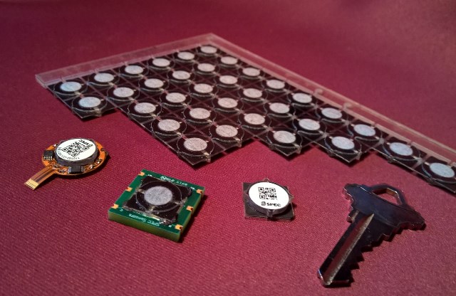
Most importantly, sensors that are manufactured as flexible or printed/flexible components can be sold in non-flexible packages (fig. 4 ) to replace existing non-P/F sensors. The P/F companies mentioned in last month’s article all stated that their P/F solutions had performance advantages over the “classical” three-dimensional versions. Joe Stetter, founder and CTO of Spec-Sensors (www.spec-sensors.com) who produces gas sensors stated it succinctly… “It is an issue of electronics vs chemistry! In physics/electronics we are concerned about the movement of electrons, vs that of ions in chemistry, and electrons move near the speed of light and are 10,000-times-or-more lower mass! So printed structures, [which] are smaller and reduce mass-transport effects, enhance the performance of the printed chemical sensors!” It thus makes good sense to address the functionality of the sensor, irrespectively of its format (that is, printed/flexible versus discrete package) and how it satisfies the requirements of the design engineer from a specification, size, and cost perspective. So, as the architect John Louis Sullivan once remarked, “Form must forever follow function.” And P/F sensors can shift form.

Fig. 4: The small 15x15x3.8-mm electrochemical gas sensors shown before-and-after singulation; packaged with analog flex interface; and as a hand-solderable assembly make integration into standard pcb and flexible hybrid platforms possible. (Courtesy: Spec-Sensors)
Chris Salthouse, co-founder of the Center for Personalized Health Monitoring at UMass, states that “sensors, antennas, and actuators all frequently require large areas to effectively interface with the world. Fabricating these devices on flexible substrates has advantages, both because the finished product can conform to complex shapes and because it enables low-cost, high-rate, roll-to-roll production. The transistors required for computation, memory, and radio communications need to be small and high-performance, so today those transistors are best fabricated in traditional CMOS processing. Our current strategy at UMass is: optimize the integration of these small rigid CMOS components with large flexible substrates that contain sensors, antennas, and actuators. We are actively working to improve the performance of transistors fabricated on the roll-to-roll process to reduce the size and number of connections to the CMOS in the future, with the ultimate goal of building systems that are entirely fabricated on a roll-to-roll process.”
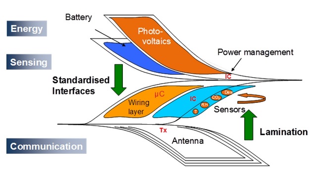
Prof. Christoph Kutter and his team at Fraunhofer EMFT, through its participation in the EU Interflex Project along with several collaborators, is vigorously addressing this important topic (fig. 5 ). [6] Fraunhofer ENAS is also pursuing high volume R-2-R manufacturing and integration issues, as is Fraunhofer IZM.

Fig. 5: This conceptual sketch of the demonstrator developed by Fraunhofer EMFT for the INTERFLEX project shows three layers of different electronic functionalities: photovoltaics and energy storage, micro-controller IC and sensors, and wireless communication. The system was built using aligned, 3D-stacking of the film layers, in a process that combines hybrid component assembly and printing techniques.
For U.S. electronic companies who hope to participate in the P/F market, there is a special concern. From 2004 to 2016 period, foreign governments have been spending substantial amounts on P/F electronics. For that period, total government expenditures will amount to $658M in Europe and $474M in East Asia. In the U.S., government investment in the same time frame will be a mere $176M – considerably less than half Europe’s and East Asia’s outlay [7, 8] . This discrepancy could have a detrimental impact on future competitiveness of U.S. technology firms.
Want to know more?
Roger Grace will make presentations on P/F sensors this year at MEMS Industry Group (MIG) Executive Congress (Napa Valley, CA, Nov. 4-6), the Sensors Global Summit (La Jolla, CA, Nov. 10-11), and Flex 2016 (Monterey, CA, Feb. 29 – Mar. 3, 2016).
REFERENCES
[1] R. Grace, “Printable/flexible sensors: valuable additions to the designer’s toolkit,” Electronic Products , June, 2015, pp. 26, 28.
[2] A. Busnaina, “Nanoprinting Scales Up,” The Wired World in 2015 , Wired Magazine Annual Briefing, p.28.
[3] A. Bandodkar et al., “Tattoo-Based Wearable Electrochemical Devices: A Review,” Electroanalysis 2015 , Wiley-VCH Verlag GmbH and Co., pp. 562-572.
[4] The Flexible Electronics Opportunity , National Research Council of the National Academies, The National Academies Press, Washington D.C., 2014.
[5] R.Grace and M. Maher; “Why MEMS-based systems solutions?,” Electronic Products , February 2011, pp. 17-19.
[6] K. Bock et al, “Multifunctional system integration in flexible substrates,”
Proceedings of the 2014 IEEE 64th Electronic Components and Technology Conference , May 2014, pp.1482-1487.
[7] Z. Kay, C. Curling; “Printed Electronics: Analysis of Competency Matrices for UK and Germany,” UKDL Newsletter, Winter 2008/2009.
[8] Dial-Up Sensors: Printed, Flexible and Organic Sensors for the Things in the Internet of Things , Lux Research, September, 2014.
About the author
With a background that includes over 45 years in high-frequency analog circuit design, application engineering, project management, and product marketing, Roger H. Grace (rgrace@rgrace.com) is the President of Naples, FL-based Roger Grace Associates, which he founded in 1982 to provide strategic marketing consulting in high tech. A MEMS pioneer, Mr. Grace has advised technologists and top executives on sensor and IC design, development, and commercialization at clients that include the international “Who’s Who” of corporations and government agencies. He received his BSEE and MSEE (as a Raytheon Fellow) from Northeastern University and was that school’s 2004 Engineering Alumni of the Year.
Advertisement
Learn more about Roger Grace Associates


