Packaging alternatives for powering the heart
CRM designers look to metal TSV, flex die stacking, and PSOI packaging technologies for high-voltage applications
BY TOM ZEMITES
Microsemi, Scottsdale, AZ
http://www.microsemi.com/
It is entirely possible that many of us may find ourselves with one or more electronic devices implanted into our bodies during our lifetime; one of the most likely is a cardio rhythm management (CRM) device.
Four main issues confront the designer of CRM devices: reliability, performance, size and cost. These issues become especially troublesome when dealing with high voltages used in implantable cardioverter defibrillators (ICD), which are generally greater than 700 V. Discrete power devices such as rectifiers, MOSFETs, SCRs and IGBTs are needed to condition, switch, and protect when providing the high voltage shock required during the defibrillation process. Zener rectifiers and MOSFETs are used to protect the CMOS control electronics from both internal and external voltage spikes. This article will focus on power management packaging options that address the issues of reduced board space, improved performance and overall manufacturing cost savings while maintaining the reliability and the performance needed in life critical applications.
Challenges in ICD packaging
The high-power devices used in ICDs impose unique design challenges. First, a large die size is required to handle power — at times greater than 700 V with surge currents up to 60 A. Second, electrical contact is needed on both the top and bottom of the device because many power devices utilize a “vertical” manufacturing structure that allows for higher blocking voltage in conjunction with higher currents. Third, high voltage arcing must be controlled. Chip and wire is still commonly used in implantables to connect the top side contact to the printed circuit board. Although chip and wire is one of the most cost effective methods, it creates other problems. A protective coating is critical to preventing arcing. Wirebonding using heavy wire can crack the die. Die and wire spacing requires additional board space. To overcome these shortcomings, one solution is creating a planar flip-chip power package that eliminates arcing, coatings and wire bonds while minimizing board space and lowering costs.
One method of creating a planar flip-chip power package is to attach the die to a ceramic carrier which brings the backside contact to the front. The ceramic carrier is shaped like an inverted “L”. The die is soldered or epoxied onto the ceramic. Metal traces are then imbedded into the ceramic which routes the backside contact to the front side forming a planar device. Solder bumps are placed on both the die and the carrier to allow for planar flip-chip attach. Board space savings versus chip and wire is greater than 10%. Moreover, ceramic is a good insulator against high voltage arcing; so depending on the component placement, coating may not be needed. There is also the added cost of the ceramic and yield lost attaching the die to the carrier due to x, y, and z planarity issues. The end result is a very reliable package, smaller space, but at a higher price.
TSV and sizing solutions
To eliminate the planarity issues created by the carrier, the use of metal filled through-silicon vias (TSV) may be a solution to bring the backside contact to the front. To do this, the die size is expanded to include non-active silicon adjacent to the active silicon region. A channel is created through the non-active silicon by first creating a hole through the silicon and then filling the hole with metal (see Fig. 1 ). Current can flow from the active region, through the backside metal and down the metal TSV. This allows the backside contact to be moved to the front side. The die size grows, but not as much as when a ceramic carrier is used, space savings will be greater than 20% versus chip and wire. All wire bonding is eliminated making for a very reliable package.
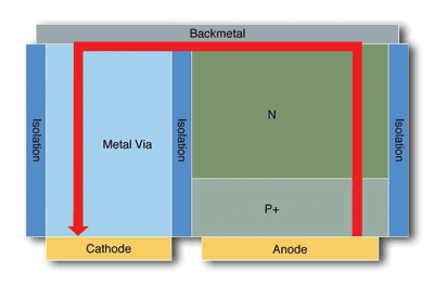
Fig. 1. Metal plated through-silicon vias (TSV).
Today’s wafer processing cost for TSV may be an issue based on observations made by VLSI Research at the recent International Interconnect Technology Conference (IITC). According to VLSI, “high-volume TSV is still some years away.” Until high-volume is achieved, per-wafer processing cost will remain prohibitively high. Therefore, the industry is experimenting with lower cost TSV solutions specifically for power devices. One can envision several variations from the basic structure that allow for die stacking. If a lower cost TSV can be realized, this concept provides a reliable, smaller solution over chip and wire.
Power die stacking is another viable option to gain size advantage. It requires starting with two or more known-good die (KGD) and vertically soldering them together. These designs use well established techniques including interposers, soldering, and wirebonding to vertically integrate the die functions. The major advantages are it requires half the board space and allows mixing of wafer process technologies. The major disadvantages are wire bonds, coating to prevent voltage arcing, and costs due to cumulative yield loss.
Another die-stacking method is folded-flex circuits, which uses origami-like folding methods. With folded-flex circuits, the power die can be flipped upon each other. The challenge for engineers is how to make contact on both the top and bottom of a power die without wire bonds, while maintaining a low profile. By molding the package, arcing can be prevented. Cumulative yield losses tend to drive costs higher, but yields will be better than soldered stacked die. Again, board space savings will be greater than 50%.
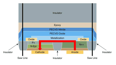
Fig. 2. Power silicon on insulator (PSOI).
Another alternative is a new hermetic packaging technique which provides reliability, size and cost advantages over existing solutions called Power Silicon on Insulator (PSOI). PSOI is a sealed chip scale package that takes a different approach to bringing the electrical connections to the same side (see Fig. 2 ). PSOI develops the active regions on the same side using standard processing steps but joins the regions with a top metallization. The top side is then sealed and protected by attaching a top side insulator. External metalized contacts are developed on the bottom of the device much like a flip-chip package, but with PSOI the bottom and sides are insulated which forms a unique “wafer level package”. The die can then be sawn in any form, single, duals, quads, etc. The concept eliminates any back-end manufacturing steps. After sawing in wafer form, simply test and ship the product in suitable containers such as waffle or gel packs for automatic pick-and-place.
Top, bottom, and side insulators isolates the junction from environmental contaminates and moisture sensitivity. The process eliminates wire bonds and protective coating, reducing overall chip size. PSOI can be manufactured with top contacts for stacking. It provides excellent thermal characteristics and provides small size while maintaining surge performance. This process provides die-to-die electrical isolation and reduces parasitics. Overall yields have to be on par with standard wafer yields to match costs. Depending on the technology, overall circuit footprint can be reduced 20% to 55%.
Miniaturization, performance, and quality are today’s leading technological challenges for today’s implantable medical design engineer. Power device size reduction simply cannot be solved with the next-generation lithography node. What’s required is advanced 3D circuit packaging plus flip-chip stacking on flexible substrates, using a new chip-scale package that can handle high voltages and bring contacts to the same surface. The most promising options are metal TSV, flex die stacking and PSOI packaging technologies. ■
Advertisement
Learn more about Microsemi


