Packaging faces a ‘perfect storm’
Electronic device packaging is changing rapidly to meet demands for higher performance in less space for rough apps
BY RICHARD COMERFORD
Editor, Electronic Products
In many ways, it's a “perfect storm” — a situation in which a set of factors combine to create your worst nightmare. In electronic design, those factors have been coming together for the last decade until, now, we are at the point where industry must change course dramatically to avoid disaster. This new direction requires that designers rethink the way devices are assembled and encapsulated if they are to meet the requirements for the next generation of not only consumer goods, but of many military and industrial applications as well.
Critical factors
This past summer, Thomas S. Tarter, the founder of Package Science Services LLC (pkgscience.com) at the Thermal Design Center in Santa Clara, CA, in which he clearly delineated the critical factors the industry was having to deal with. For one, he noted, there were problems in continuing to follow Moore’s Law by shrinking transistor size; he stated that, “Limitations to transistor gate size are an issue in the future, and interconnect losses pose a serious problem for high speed chips now.”
Another factor he points too is the proliferation of powerful mobile devices that test the limits of density and performance in compact systems — in short, more power in less space. At the same time, there is the cost factor; suppliers must reduce, or at worst maintain, cost while providing greater functionality.
These factors not only apply to established, IC-based components but to new types of devices such as MEMS-based systems. Eric Mounier, a project manager at market research firm Yole Développement, in a recent report on MEMS manufacturing and packaging, points out that although MEMS technologies have not been subjected to the same size demands as ICs, they are still under pressure to shrink in size, increase performance, and hold the line on cost.
Stacking up
There are several things that can be done, separately or together, to deal with these issues (see Fig. 1 ). These changes will typically involve the use of new materials, processes, and assembly techniques.
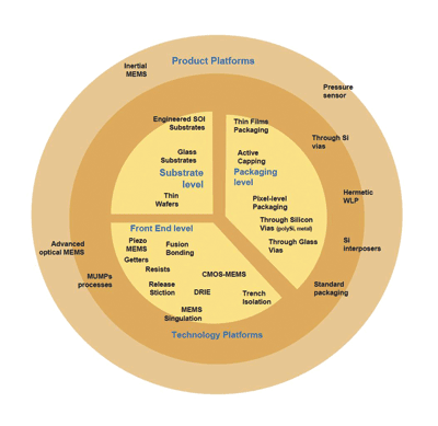
Fig. 1. In its February, 2011, report “MEMS Manufacturing & Packaging,” Yole Développement examines the technology trends shown in chart above. Many on these trends are also part of non-MEMS device fabrication as well.
One of the first approaches is to go from the traditional 2D assembly, in which all the electronic devices in a package are on the x-y plane, to a 3D technique, in which elements exists in the z plane as well. The common way to accomplish this is to stack die on top of each other and interconnect them.
In the simplest case, the individual die can be connected to each other using wire bonding from the pads on the edge of one die to pads on the edge of another, or to pads that have been made on a device-supporting substrate (see Fig. 2 ). Spacers may be used between the die to separate them. The approach depends on using more-traditional wire bonding as the means of interconnection. Because it relies on wire bonds, however, this packaging approach, often referred to as system in package (SiP), is seen as not completely integrating the chips into a single circuit.
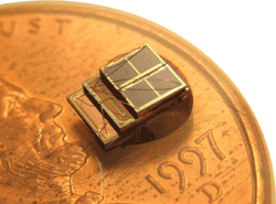
Fig. 2. In this wireless identification and sensing platform (WISP) node developed at the University of Michigan’s Wireless Integrated Microsystems Laboratory (WIMS), solar cells (top layer) and a battery (bottom layer) are wire bonded to the middle layer, which has a processor, SRAM, and a PMU.
To achieve tighter integration, some manufacturers have turned to a number of other stacking approaches wafer-on-wafer, die on wafer, and die on die that rely upon through-silicon vias (TSV).
As it’s name implies, a TSV is an electrical connection (via) made by passing conducting material vertically through the silicon wafer (see Fig. 3 ). This can shorten the interconnection / signal path between circuits and thereby permit at higher speeds. Tessera (www.tessera.com) was one of the first companies to develop commercial TSV, which it licenses as manufacturing IP.
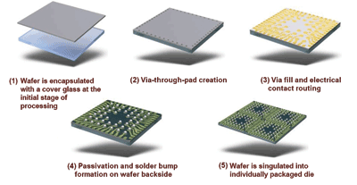
Fig. 3. Tessera originally developed its ShellCase TSV technology shown above for use in imaging devices.
Using TSV technology, it is possible to build components are built using two or more semiconductor wafers, each with different types of etched circuits. The wafers are then carefully aligned so that the circuits on each wafer match with their counter parts on the other wafer and their TSV connect precisely. The wafers are then bonded and diced into 3D ICs. It is also possible to create TSV once the wafers have been bonded.
The wafers used in this process can may be thinned, removing excess silicon in the substrate that is not functionally required. This further reduces the volume of the resultant IC stack.
Their are two variation on this wafer-on-wafer construction technique. In one, die-on wafer, one of the wafers is first cut into die and individual die are attached to their counterparts on an undiced wafer. This approach is particularly useful when the die sizes are dissimilar. In the other, die-on-die technique, all wafers are cut into die and the individual die assembled.
Benefits and challenges
As previously alluded to, this approach to IC stacking offers numerous benefits, including:
• Putting more functionality into less space, thereby perpetuating Moore’s Law.
• Using TSVs reduces the signal paths and therefore propagation delays, so devices can operate at higher speeds.
• Having shorter, direct signal paths also result in lower power consumption, which results in less heat and longer battery life.
But the approach also has its tradeoffs. While the ability of tightly integrating stacks of ICs presents new design possibilities, design complexity can likewise increase, and designers will need EDA tools that are 3D aware to make the best of 3D possibilities.
The opportunity to cut costs with stacking is a double-edged sword. On the one hand, partitioning a design into smaller pieces that are fabricated separately could improve yields and cut cost. On the other hand, assembly costs can rise.
Stacking die also frees designers form having to use a single IC process line to create a device, and thus bring the best technologies to bear to realize the end device. This is a particular benefit for MEMS devices, allowing MEMS die to be combined with standard CMOS logic. However, this means managing multiple process and can make the supply chain more complex.
Not to be overlooked is the fact that TSV lend themselves to multiple, wide buses, which can greatly increase data throughput. But this may come at a cost in design complexity and nonstandard implementation of data paths.
Packaging the future
While changing the way devices are packaged and assembled can be very challenging, the rewards of doing so seem worth the effort.
A recent development by Symmetricom (www.symmetricom.com; see http://tiny.cc/a80be) is a case in point. Working under a program initiated by the U.S. Defense Advanced Research Projects Agency (DARPA) to create a chip-scale atomic clock, the company developed a number of advanced fabrication and packaging techniques. For the so-called physics package (see Fig. 4 ), the company developed a tensioned polyimide suspension, microfabricated a silicon vapor cell, developed a low-power vertical-cavity surface-emitting laser (VCSEL), and created a technique for on-line vacuum packaging fabrication to eliminate convection/conduction.
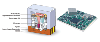
Fig. 4. The chip-scale atomic clock created by Symmetricom under a DARPA uses highly advanced fabrication and packaging technology.
This entire package can operate on 10 mW, opening up an array of applications that could not be addressed with the technology previously available. While the current implementation is aimed at high-end, big-ticket applications, who knows where new packaging techniques could put this technology tomorrow? ■
Advertisement
Learn more about Electronic Products Magazine


