By Jan Vardaman (TechSearch International) and Dan Tracy (SEMI)
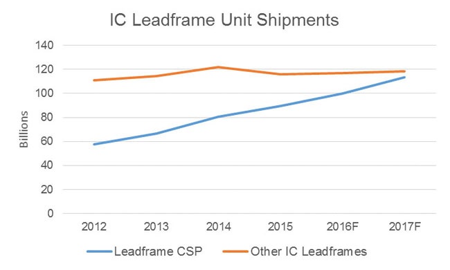
While much of the recent attention has been focused on the growth of wafer level packages (WLPs), specifically fan-out WLPs, this is not the only segment forecast to undergo strong unit growth. In total, IC leadframe shipment growth will trend in the low single-digit range; the growth is entirely attributed to the chip-scale package (CSP) leadframe form factor. Combined, the more traditional IC leadframe segments are expected to experience flat shipments trends, while leadframe CSP shipments continue to growth.

Source: SEMI and TechSearch International, Global Semiconductor Packaging Materials Outlook
Leadframe CSP packages find broad adoption in analog, power, mixed signal, general purpose logic, sensors, and other device applications. A number of leadframe CSPs are in the form of quad flat no-lead (QFN) packages. These packages have pads instead of leads and do not use solder balls. QFNs are found in mobile phones including smartphones, toys, games, tablets, medical systems, industrial, computers, networking, and automotive products. Devices packaged in QFNs include many different MEMS and sensors such as accelerometers, gyroscopes, magnetometers, and pressure sensors, and power management devices, controllers, and ASICs. Stacked die versions are increasingly common. Gyroscopes and accelerometers are stacked with wire bonds in the QFNs found in many wearable products. QFNs are also increasingly common as packages for automotive electronics.
This form factor will grow as it delivers a thin, small, and low-cost solution required in many applications. Emerging in the market are coreless structures based on a modified leadframe technology called a Molded Interconnect Solution/System (MIS) that deliver higher I/O and SiP solutions. Advancements are needed to further the high-volume ramp of MIS and other routable-leadframe CSP technologies.
Small package form factors deliver solutions needed in mobile applications and will provide the package technology for many sensor and wearable applications emerging in the market place.
The information in this article is from the Global Semiconductor Packaging Materials Outlook—2015-2019 report produced by SEMI and TechSearch International. In developing this report, over 150 in-depth interviews were conducted with semiconductor manufacturers, packaging subcontractors and packaging materials suppliers throughout the world. The report provides coverage of material segment market size, regional market size, supplier market share, and more.
TO ORDER YOUR COPY of Global Semiconductor Packaging Materials Outlook—2015 to 2019 report, please contact Dr. Dan P. Tracy, research development director, Industry Research and Statistics, SEMI via email at dtracy@semi.org, or telephone 1.408.943.7987 or click here for sample, pricing, and ordering information.
For all the latest news, please follow SEMI on LinkedIn and Twitter.
Global Update
SEMI
www.semi.org
April 5, 2016
Advertisement
Learn more about Electronic Products Digital


