When considering the long term reliability of a PCB, you must take into account the vias that you have on your board. While an invaluable and essential part of board design, vias introduce weaknesses and affect solderability. This article will discuss PCB reliability through vias, the potential concerns that are introduced into your board through their implementation, and how to minimize those concerns to acceptable levels.

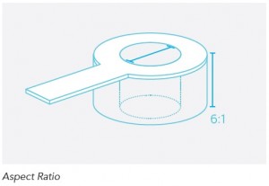
The first rule for via design is simple: bigger is better. Larger vias have greater mechanical strength as well as greater electrical and thermal conductivity. While space is always a consideration when it comes to PCB design, vias should have large drill holes with large aspect ratios. While manufacturers can achieve drill holes significantly smaller than this, 20 mil drill width with an annular ring of 7 mil and an aspect ratio of 6:1 should be used if space allows. For many boards this may be an unachievable goal, requiring drill holes in the realm of 8 to 12 mils, or even smaller.
Check with your manufacturer to establish what their capabilities are. However, even if they are capable of providing smaller, the basic premise of bigger is better stands true. When a PCB is exposed to thermal changes in its processing or in its end working environment, the varying coefficient of thermal expansion (CTE) between the laminate and the copper can cause issues. PCBs are constrained through structural latticework to limit horizontal expansion but can expand and contract significantly in the vertical direction. As copper expands and contracts at slightly less than one fourth of the rate of FR-4 laminate, vias are literally being pulled apart every time the board is heated. If the board is too thick and the copper in the via too thin, then the board will expand too much and the copper will break, literally tearing the via apart. In the example above, to get the appropriate aspect ratio with a drill width of 20 mil, this would result in a total pad diameter of 34 mil and allow a max board thickness of 120 mil.

Size is important with vias, but location is tantamount. If a via is located close to a solder pad,
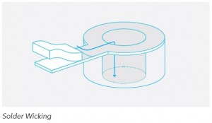
a myriad of problems may arise. Foremost is the problem with solder wicking. As the via heats up, it pulls the solder from the solder pad, through the via, and onto the other side of the board, leaving the pad either solder deficient or completely solder free. The larger the via, the more solder will likely wick away, making it less likely that you will have a solid mechanical and electrical joint. Fortunately, this concern can be fixed by any of three no-cost methods.
Providing a solder mask between the lead and the via creates a barrier to the movement of the solder. This is a simple yet effective method, though it does have its drawbacks. Due to the minimum width required for a solder mask, this may require the via to be moved even farther from the lead. The distances required may seem minimal, in the 2 – 5 mil range, however, when space is at a premium or the board is carrying high frequency signals, this may have a profound effect on your design. However, when these aren’t issues, this is a great way to avoid the solder wicking concerns.
If there is no space to move the via and you need to minimize the via size, it is possible to use an encroached or tented via. By masking the via pad, you save space and also make it possible to silkscreen over the via. However, this makes it impossible to use the via as a test point as the copper will no longer be accessible from the side that is tented. At this point, you need to make a decision on whether an encroached or tented via is best. A tented via is completely sealed and will create a better surface for silkscreening as well as a better barrier against contamination. This barrier works both ways, though. If a via is tented on both sides of the board, contamination can fill the void during the board construction. At elevated temperatures, such as when the PCB is being reflowed or wave soldered, the contamination can outgas and destroy the via and thus the board. When you tent a via, make certain you only do it on one side. An encroached via eliminates this issue by keeping the hole itself open and also has the added benefit versus a tented via of being possible no matter the via size. While tented vias need to be small enough for the solder mask to bridge the drill hole, the encroached via only covers the annular ring and can be as big or small as needed.
Filled vias are also an option, which increase strength, electrical/thermal conductivity, and protect the via from solderwicking and contamination. The main drawback to filled vias is that they can add significant costs to the board. The other methods should have no impact on cost whatsoever.
Every design has different requirements and constraints. However, when possible, utilize these tips by using the largest vias, the appropriate aspect ratio, and by thoughtfully choosing the solder masking style that suits your needs. This will help reduce the overall lifetime costs by increasing reliability of your products.

Advertisement
Learn more about Advanced Assembly


