It’s not uncommon to envision massive room-sized machines when thinking about particle accelerators. After all, CERN, the most famous of the lot, takes up miles worth of space. But the truth is, particle accelerators come in all shapes and sizes, not just gargantuan. An international team made up of physicists at SLAC/Stanford and German’s Friedrich-Alexander University are looking to shrink them down to chip to the size of a microchip component.
Their goal is to “do for particle accelerators what the microchip industry did for computers,” explains SLAC National Accelerator Laboratory physicist Joel England, alluding to the tech’s potential in medical therapy, x-ray imaging, and security scanners to name a few. A prototype is already in the works, building off prior experiments both that both institutions have already begun.
There are multiple schools of thought on how to miniaturize the particle accelerator. The primary approach relies on plasma wakefield acceleration, a technique which accelerates electrons to very high energies over a few centimeters by firing intense short pulses of laser light into clouds of ionized gas (plasma), creating a rippling effect through the plasma that leaves behind charged particles in its wake, similar to how speed boats ruffles the top layer of water as they move forward. Next, a second laser pushes extra electronics into the plasma, gaining acceleration as they move through the wake.
Theoretically, the miniaturized accelerator-on-chip would employ a similar technique, but within a vacuum. Instead of relying on the ionized gas to provide structure the way the plasma Wakefield concept dictates, the accelerator-on-chip would build structure out of a dielectric optical material — an insulating material that’s a poor conductor of electricity.
According to a 2013 report published in the journal Nature , a prototype of this sort was successfully created using laser to accelerate electrons through a line of nano-structured silica glass chips. Unlike SLAC’s own prototype, it accelerated electrons to near light speed within a microscopic channel that measured less than 1/200th of a human hair. By etching nanoscale-sized ridge patterns along the channel’s walls, the scientists were able to increase the positive electric field and provide electrons with a boost of energy that outweighs the energy lost moving through the channel.
Later that year, German physicist Peter Hommelhoff achieved nearly identical results without needing to boost the electrons to near light speed.
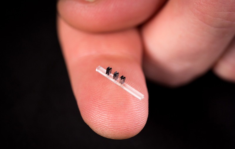
SLAC’s Joel England believes that everything in these two experiments can be made using micro-fabrication, creating each separate stage of the accelerator on a single silicon wafer. At this point, the key to achieving higher and higher energy is to simply stack them in succession, similar to how conventional accelerators use a succession of metal cavities to reach energy levels. “But our first goal is just to develop all the components and then figure out how to integrate them using a single set of fabrication steps on a single wafer,” England tells Gizmodo.
England and has team have received a $13.5 million grant from the Gordon and Betty Moore Foundation to pursue their research.
Source: Gizmodo
Advertisement
Learn more about Electronic Products Magazine


