By Maurizio Di Paolo Emilio, editor-in-chief, Power Electronics News
Devices equipped with power management ICs (PMICs) tend to be smarter and more efficient, as they regulate the flow of energy from the inside and the outside of the device. PMICs help these devices use power more efficiently while extending their life. Therefore, the demand for such components is increasing rapidly.
One of the most critical factors in an FPGA-based system is power management. Powering an FPGA requires careful system analysis, and the same technique can almost always be used for an ASIC.
Engineers spend most of their time programming and don’t want to waste time and energy thinking about designing the right power supplies. In fact, the best approach to power delivery is to use a robust, flexible, and tested design that meets the requirements and can be scaled with the design.
The voltage that supplies the FPGA core is subject to wide current variations characterized by extremely high slew rates. This requires the controller to be able to deliver current steps to the load while minimizing changes in its output voltage.
Multiple power rails, power-up sequencing, tight tolerances, transient response, system reliability, total solution cost, and size — these are things that designers are concerned about when powering an FPGA. One way to address these challenges is to use a reference design.
Most recently, Renesas Electronics released three PMIC reference designs for powering the multiple supply rails of Xilinx FPGAs. The reference designs allow for easy management of rail feeding in the Xilinx Artix-7 FPGA, Spartan-7 FPGA, and Zynq-7000 SoC systems. Based on multi-phase PMICs, Renesas’s BGA-packaged solutions offer easy-to-use turnkey solutions that allow a single project to support different degrees of Xilinx speed and DDR memory types such as DDR3, DDR3L, DDR4, LPDDR2, and LPDDR3.
The three reference designs — ISL91211A-BIK-REFZ, ISL91211A-BIK-REFZ, and ISL91211AIK-REFZ — are based on Renesas’s ISL91211AIK and ISL91211BIK PMICs in BGA packages.
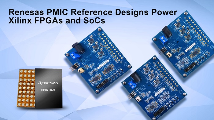
The ISL91211A-BIK-REFZ reference design board for Artix-7 devices employs the ISL91211AIK and ISL91211BIK multi-phase PMICs, ISL80030 3-A synchronous buck DC/DC converter, and ISL21010DFH312 micropower voltage reference. The PMICs deliver efficiency up to 95% for multiple power rails and they accept 5-V input from a plug-in AC/DC adapter or DC power supply. The ISL80030 supports VCCO and VCC_IO for 3.3 V, 2.5 V, and 1.8 V, and the ISL21010DFH312 is for an XADC input voltage of 1.25 V with ±0.2% accuracy.
The ISL91211BIK-REF2Z reference design board for Spartan-7 devices uses the ISL91211BIK multi-phase PMIC and ISL80030 3-A synchronous buck DC/DC converter. The ISL91211BIK is required for VCCINT, VCCBRAM, VCC_DDR, VCCAUX, and VTT, and it accepts 5-V input from a plug-in AC/DC adaptor or DC power supply. The ISL80030 DC/DC converter supports VCCO and VCC_IO for 3.3-V, 2.5-V and 1.8-V rails.
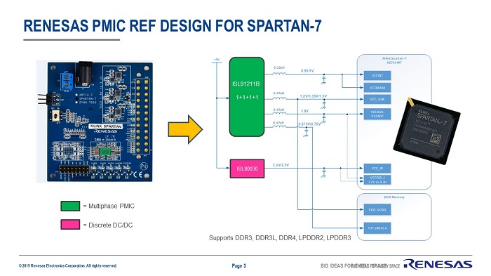 Fig. 1: Reference design for Spartan 7 (Image: Renesas)
The ISL91211AIK-REFZ reference design board for Zynq-7000 devices utilizes the ISL91211AIK multi-phase PMIC, ISL9123 low-Iq buck regulator, and two ISL80030 3-A synchronous buck DC/DC converters. The ISL91211AIK is required for VCCINT, VCCBRAM, VCC_DDR, and VCCAUX. The ISL9123 supplies the VTT power rail, and two ISL80030 DC/DC converters support VCCO and VCC_IO for 3.3-V, 2.5-V, and 1.8-V rails.
The solutions can provide a total output current of up to 20 A and are equipped with independent dynamic voltage scaling, effectively accelerating the development of power supplies for a variety of industrial applications such as motor control, machine-vision cameras, and programmable logic controllers (PLCs). Their tuned control feedback optimally supports the load profiles of Xilinx FPGAs and can internally manage on/off sequencing without additional algorithms. They also may be used in home gateways and appliances, portable medical devices, and wireless equipment.
The application of a 2-MHz switching frequency and fast load transient response allows each PMIC board to use 22-µF output capacitors and a small inductor to reduce the size of the solution. PMICs are available in 4.7 × 6.3-mm, 35-ball BGA with 0.8-mm-pitch packages.
Both multi-phase PMICs offer Renesas’s R5 modulation technology, which allows for extremely fast transients and can dynamically change output voltages to improve system performance and efficiency. The R5 controller technology is a proprietary modulation technique that offers the fastest response to changing output load conditions, according to Renesas.
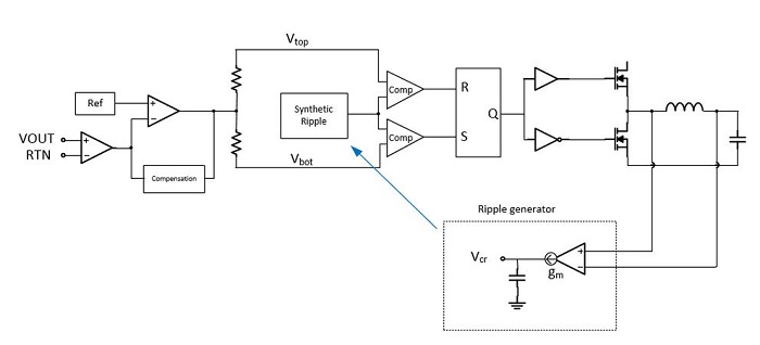 Fig. 2: Simplified diagram of Renesas’s R5 technology (Image: Renesas)
Renesas calls the R5 technology the next evolution of its unique current-mode hysteretic controller with improved bandwidth and lower Iq than previous implementations.
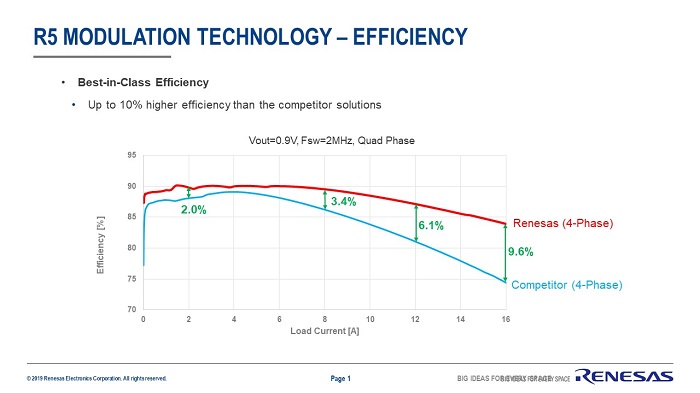 Fig. 3: Efficiency of R5 modulation technology (Image: Renesas)
The R5 modulator operates using a hysteretic window and a synthetic current signal labeled in Fig. 4 as Vcr. The synthetic ramp is a representation of the inductor waveform without needing to directly sense the inductor current.
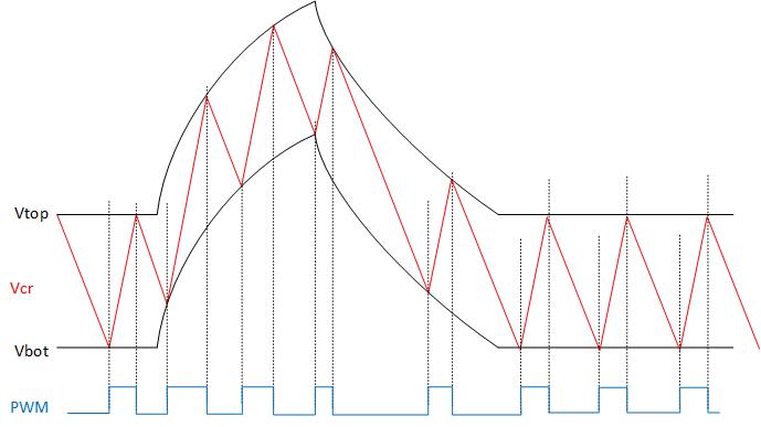
Fig. 4: R5 controller in transient condition (Image: Renesas)
In steady state, the window is controlled with the aim of having a constant switching frequency with a constant duty cycle. The position of the window allows the loop to react to a dynamic load better than a fixed-frequency modulation scheme. The R5 modulator increases the efficiency of the load through a current play in the MOSFET.
Also, the R5 modulator does not rely on a fixed clock to set or reset PWM pulses. Therefore, it can, of course, skip the pulses when necessary. When the load current is very light, the switching frequency of the loop is lowered, drastically reducing switching losses.
All of the reference design boards are supplied with a user’s guide, complete schematic, bill of materials, and PCB layout files. They are available through Renesas’s distribution network.
Advertisement
Learn more about Electronic Products MagazineRenesas Electronics America


