Power electronics for solar power inverter systems
Here are the properties of power semiconductors that you must consider to get the highest efficiency in solar inverter applications
BY WOLFGANG FRANK
Infineon Technologies AG
Milpitas, CA
http://www.infineon.com
Use of photovoltaic systems to generate electricity in homes and businesses is becoming increasingly popular, as the cost of conventional electric energy increases while the cost-effectiveness of solar power systems improves. While much attention is paid to gradual improvements in the efficiency of solar cells, steps can also be taken to improve the efficiency of the power conversion electronics of the system. Solar electric systems incorporate inverters or power control units that transform the dc electricity generated by the solar cells into ac to run appliances or sell to a utility grid. An intelligent setup and the use of the most advanced power semiconductor technologies are keys to the highest inverter system efficiency.
The cells that form a solar panel are connected in series into strings, with the positive electrode of one cell connected to the negative electrode of the next cell. Each string is connected to a diode to prevent power loss in case one of the solar cell strings is shorted, and to prevent reverse charging. Each string is also connected to a common, specified dc link through its own power conditioning circuitry, which includes a dc/dc boost converter to increase the voltage from the cells to the specified dc link level. In the most common topology used today, called multistring, the dc output of each converter is fed into one inverter, which converts it into an ac voltage that is fed into the main power grid (see Fig. 1 ).
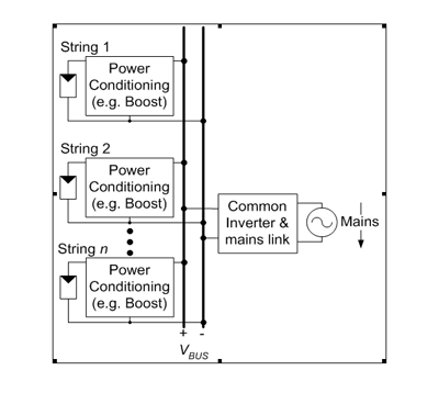
Fig. 1. Solar inverter in multistring configuration.
Grid-connected inverters must generate clean waveforms with minimal harmonics, and not degrade the power quality of the existing utility grid. In many cases, therefore, the inverter function is coupled with a “mains link” consisting of a transformer and output filter. The transformer blocks any dc component from the main grid. While the transformer causes a marked efficiency drop, on the order of 1% to 2%, the inverter must avoid dc components, so the sacrifice is commonly made. Table 1 shows an estimation of the contribution of each stage to losses, size and system cost.

Table 1. Estimation of contributors to losses, system size and cost in a multistring solar power system
Clearly, the transformer is one of the main contributors to losses and cost. There are systems available that do not use a transformer, depending on the legal requirements of the country in which the solar inverter is sold, and these provide higher efficiency. However, the transformer is mandatory in many countries, and this isolation function is therefore outside the scope of this discussion.
The output filter attenuates the current ripple that is generated by the output inverter stage. The size and cost of this filter are inversely proportional to the switching frequency of the inverter; i.e., the higher the switching frequency, the smaller and cheaper the filter. This relationship requires a trade-off with the reality of hard switching conditions, in which a higher switching frequency increases losses and lowers efficiency. It has been found that a value of between 16 and 20 kHz will meet the demand of systems with low audible noise and high efficiency, but the specific design of the filter is also outside the scope of this discussion.
The power electronic stages that perform the dc/dc boost and dc/ac conversion functions have a major impact on the conversion efficiency of the inverter. Modern power devices have been designed specifically to minimize losses, and include such devices as punch-through (PT), non-punch-through (NPT) and trench-insulated gate bipolar transistors (IGBTs) that offer reduced conduction and switching losses.
Power semiconductors for the dc/dc boost converter
A typical dc/dc boost converter (see Fig. 2 ) operates at a switching frequency of approximately 100 kHz or higher in solar power applications. It is run in a continuous conduction mode, which means that the current in the boost inductor (L1) has a continuous waveform at rated conditions. The transistor (T1) charges the inductor, and the diode (D1) acts as a freewheeling diode when the transistor is turned off. This means that the diode is actively turned off when the transistor turns on again, which makes reverse recovery behavior an important consideration in efficiency.
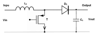
Fig. 2. Typical dc/dc boost converter.
The reverse recovery behavior of silicon diodes generates high losses in both the boost transistor and the corresponding diode. Figure 3 compares the typical reverse recovery behavior of common silicon diodes with that of a silicon carbide Schottky diode. A silicon carbide diode does not show such behavior, and there is only a capacitive undershoot of the diode current, caused by the charge of the junction capacitance of the diode. The silicon carbide diode reduces the turn-on losses of the transistor and the turn-off losses of the diode dramatically, and also reduces electromagnetic interference because the waveform is very smooth, with no oscillations. The latest generation of SiC diodes has the added benefit of significantly improved over-current and over-voltage robustness over first-generation devices.
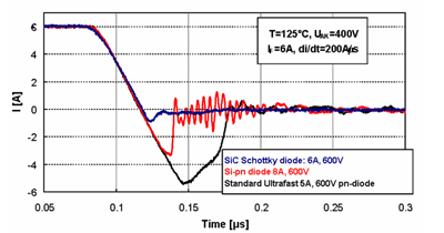
Fig. 3. Reverse recovery behavior of common silicon diodes (black, red) and a silicon carbide Schottky diode (blue)
Many techniques have been tried to avoid the losses caused by the reverse recovery of the common silicon diode, such as zero current switching and zero voltage switching. All of these techniques, however, result in an increase of the number of components and system complexity, and therefore very often lead to a decrease in reliability. With a minimum of components, the same efficiency can be achieved by using silicon carbide Schottky diodes, even under hard switching conditions.
The high switching frequency of the solar inverter dc/dc converter also requires a high-performance boost transistor. The introduction of superjunction transistors makes devices available that offer significant reductions of area-specific on-state resistance (RDS(on) ) over traditional MOSFETs. For example, as shown in Fig. 4 , the area-specific RDS(on) for such devices as the CoolMOS MOSFETs from Infineon is approximately 4 – 5 times lower than that achieved by standard technologies.
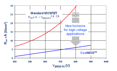
Fig. 4. Comparison of the area-specific RDS(on) of CoolMOS and common MOSFET technologies
Several investigations have shown that the use of silicon carbide diodes with superjunction MOSFETS results in solutions having superior performance over standard MOSFET and diode technology combinations.
Especially for voltages above 500 V, some manufacturers have begun to use a charge-compensation principle. This reduces the on-state resistance of the epitaxial layer as the major resistance contributor in high-voltage MOSFETs by a factor more than 5.
Power semiconductors for the inverter
The output inverter converts the dc link voltage to an ac form and connects it to the main power grid. The inverter must handle the sum of the current that is generated by all the string boost converters, but its switching frequency is not normally as high as that of the dc/dc converters, so IGBTs are ideal for this stage. Figure 5 shows the cross sections of standard NPT and trench-insulated IGBT technologies.
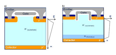
Fig. 5. Cross section of IGBT technologies: (a) Standard NPT technology. (b) Infineon TrenchStop technology.
Both technologies use thin wafer technology to reduce the conduction and switching losses that are caused by a large substrate thickness. Both illustrated technologies are non-epitaxial, which do not use epitaxial crystal growth processes, which are expensive because the blocking voltage is defined by the thickness of the grown crystal.
Standard NPT cells, including those of the “fast” generation, show a triangular electrical field inside the semiconductor during off-state. All the blocking voltage is taken over by the thickness of the n- region of the substrate, so the electric field is zero before it reaches the collector region. The chip thickness is 120 µm for a 600-V chip and 170 µm for a 1,200-V chip. The temperature coefficient of the saturation voltage is positive, so that paralleling can be easily done.
The TrenchStop technology combines advanced trenchgate and fieldstop technologies to reduce conduction losses. The trenchgate provides a larger channel width, which reduces the channel resistance. The n-doped fieldstop layer stops the electrical field at a considerably lower value of the off-state voltage. This leads to cell designs in which the electrical field can be almost horizontal in the n- substrate layer. The voltage stopping capability of the fieldstop layer can allow further reduction in the thickness of the chips, which enhances the benefits of thin wafer manufacturing. The TrenchStop technology also enables paralleling.
Table 2 shows a comparison of IGBTs for blocking voltages of 600 V and 1.200 V. The total switching energy of each transistor technology is normalized to its rated current, so that it is independent of the chip size now and a comparison of the performance is directly possible. However, it needs approximately double the current while using a 600-V device compared to a 1200-V for a system with the same output power.

Table 2. Comparison of typical values for saturation voltage (VCEsat) and normalized total switching energy (Ets) for 600 V and 1200 V IGBT technologies for a hard switching condition
Because 600-V TrenchStop devices reduce switching and conduction losses by more than 50% compared to 1200 V devices, it is important for the overall system setup to use the superior properties of 600 V technologies as much as possible. However, in 1200 V applications, switching frequency is the primary determinant as to whether Fast or the latest generation TrenchStop2 technology provides the better performance, although TrenchStop2 is more optimized for an excellent trade-off between low conduction losses and low switching losses.
The IGBT usually needs a “freewheeling” diode on which it can commutate. Traditionally, the freewheeling diode has been required to have a very low voltage drop to get the lowest overall losses. However, it has been shown5,6,7 that, depending upon application requirements, there can be other approaches to achieving even lower overall losses in the diode and in the IGBT. For example, a version of the Infineon EmCon diode has been optimized for use with 600 V IGBTs at switching frequencies of 15 kHz and above. When used at the nominal 16 kHz frequency of a solar inverter application, this can produce a higher forward voltage drop and lower switching losses.
Figure 6 shows a comparison of losses for a TrenchStop IGBT and an EmCon diode in EmCon3 technology, which is application-optimized, (left bar) and a TrenchStop IGBT with an Emcon2 diode that is optimized for low conduction losses (right bar). The yellow and orange portions of the bars indicate the conduction and switching losses, respectively, of the IGBT, and the dark blue and the light blue portions are the conduction and switching losses of the diode.
At a switching frequency of 16 kHz, a load angle of cos ϕ = 0.7 and rated current, the Emcon3 diode generates more losses during conduction (dark blue), but offsets that with a higher gain in switching performance. Furthermore, it also decreases IGBT switching losses during turn-on. There is an overall advantage of approximately 1 W in lower losses with the application optimized EmCon3 diode.
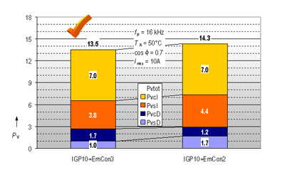
Fig. 6. Loss balance of TrenchStop IGBT (10 A/600 V) for application-optimized diode (left) and a VF-optimized diode (right).
References:
1 F.C. Lee, et al. “Performance Evaluation of CoolMOS and SiC Diode for PFC Applications”; Center for Power Electronics Systems, Blacksburg VA.
2 Infineon Technologies: IKW50N60T Datasheet; Infineon Technologies, Germany, 2006
3 Infineon Technologies: SKW25N120 Datasheet; Infineon Technologies, Germany; 2006
4 Infineon Technologies: IKW25N120T2; Datasheet; Infineon Technologies, Germany; 2006
5 W. Frank, H. Huesken. “Considerations on Design of Antiparallel Diodes for Combination of IGBT and Diodes in One Package”; International PCIM Conference 2005, Nuremberg, Germany, 2005.
6 Y. Zhou, W. Frank, Z. Chen. “New Trench Field Stop IGBT in UPS Application”; PCIM China Conference 2007, Shanghai, China, 2007.
7 W. Frank, H. Huesken, F. Hille, Z. Chen. “A new high voltage diode technology with reduced switching losses and improved softness”; International PCIM Conference 2007, Nuremberg, Germany, 2007.
Advertisement
Learn more about Infineon Technologies


