Perfect electronics power supply transforms the alternating current (AC) distributed to our homes and factories into direct current (DC) that electronics need. In a perfect world, the direct current would be noise-free or free of ripple or harmonics from the AC. In addition, the ground, which is the reference for our DC power, would be clean and pristine. As engineers, we quickly learn our world is far from perfect. That means we have to use our skill and knowledge to obtain the desired results despite the limitations.
One must first understand the operating environment and realize there is often radio frequency interference from external transmitters as well as the digital circuits operating on the same printed circuit board (PCB). Let’s start by examining the AC plug. In most cases, a powerline filter such as the one depicted in Figure 1 is desirable.
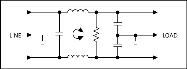 Figure 1. A common-mode choke powerline filter.
The filter serves a central purpose to symmetrically protect the device from both sides. It protects emissions from the the powerline into the device and from the device back into the powerline. It is necessary to test for emissions coming out of the box as well as testing for the susceptibility of signals entering into it.
General Layout Errors at the Board Level
In general, multilayer boards with solid ground planes and power planes produce the highest level of signal integrity.
Choosing ground star points on the chassis and on each board is a good starting point. Some inexperienced users view ground as a magical place where all bad things and interference disappears. Sometimes users start out with the ground star, but then do not bring the return currents back separately from each type of circuit to that star. Figure 2 illustrates that error.
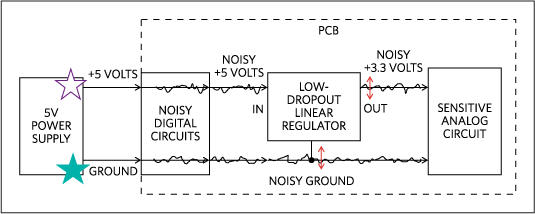 Figure 2. Ground bounce errors in a system.
We start out with a 5V power supply with a star ground. The noisy digital circuits add more noise to both the +5V power supply and the ground. We sense that an analog circuit requires a clean 3.3V voltage, but rather than running a separate wire back to the power supply for both +5V and ground to their star points, we get lazy. An LDO is needed to make a clean 3.3V power supply, or so we think. In actuality, the linear regulator always keeps its output exactly 3.3V above its reference or ground. Therefore, if the ground is bouncing up and down like the red arrow indicates and the LDO is doing its job, the +3.3V output will go up and down following the ground bounce. The question we have to ask ourselves is how many hours we will spend troubleshooting because we did not run separate analog and digital wires back to the star points? Figure 3 illustrates a better way to connect the analog circuit.
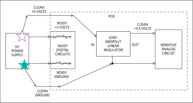 Figure 3. Proper use of the ground and power star points. This implies that power and ground are clean at the star points.
The implication that power and ground are clean at the star point (shown in Figure 3) means that power and ground are homogenous at the star points. There is no differential noise between power and ground. Ideally, the power-supply output would have a near-zero impedance or have decoupling capacitors with low equivalent series resistance (ESR) at the frequencies of interest. The individual conductors connecting the various circuits to the ground and power star points have series resistance and inductance. We rely on that resistance and inductance to isolate the noisy circuits from the clean circuits. The series resistance and inductance, as well as the decoupling capacitors at the output of each circuit block, form lowpass filters. If the wiring to the different circuit blocks is relatively short, it can become necessary to add discrete resistance and inductance.
Decoupling is complicated because capacitors have parasitic inductance. In practice, a capacitor is represented as a series RLC circuit as shown in Figure 4. The capacitance will dominate at low frequencies, but above the self-resonant frequency (SRF), the dip in each plot as shown in Figure 5, is the point where the impedance of the capacitor will begin to look inductive. Thus, a capacitor is only useful for decoupling purposes over a frequency range that is near or below its SRF when the capacitor presents a low impedance at the frequency of interest.
 Figure 4. A capacitor with inherent parasitic components.
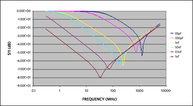 Figure 5. Capacitors with six values and their respective self-resonance points.
Figure 5 shows the typical SRF performance for various capacitor values.1 From these plots, the SRFs can clearly be seen by the dip in the graph. It also shows that the larger capacitances provide better decoupling (appear lower impedance) at lower frequencies than the smaller valued capacitors. Free SPICE programs are available for capacitor self-resonance plotting.2, 3, 4
Specific Layout Errors at the Switching Power-Supply-Integrated Circuit Level 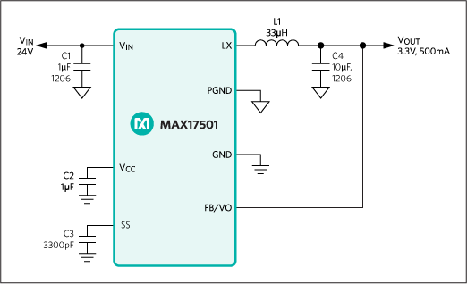 Figure 6. A simplified schematic diagram of the MAX17501 switching power supply.
In Figure 6, note the two different ground symbols (the triangles) that indicate the high-current fast-rise-time switching pulses. It is important to isolate the high-frequency, high-current pulses from the analog small-signal or reference ground.
In Figure 6, a ceramic input filter capacitor5 (C1) is placed close to the VIN pin of the device. This capacitor acts as a power reservoir to smooth the power pulses that would have been propagated back to the DC source supply if the capacitor was not present. Depending on the rise time of the switching pulses, this capacitor can be made up of several capacitors of different sizes to cover the large frequency range. The bypass capacitor for the VCC pin should also be placed as close as possible to the VCC pin. This capacitor might also need to be made of multiple capacitors. For the most efficient heat dissipation, a number of thermal vias should be provided under the exposed pad of the device.
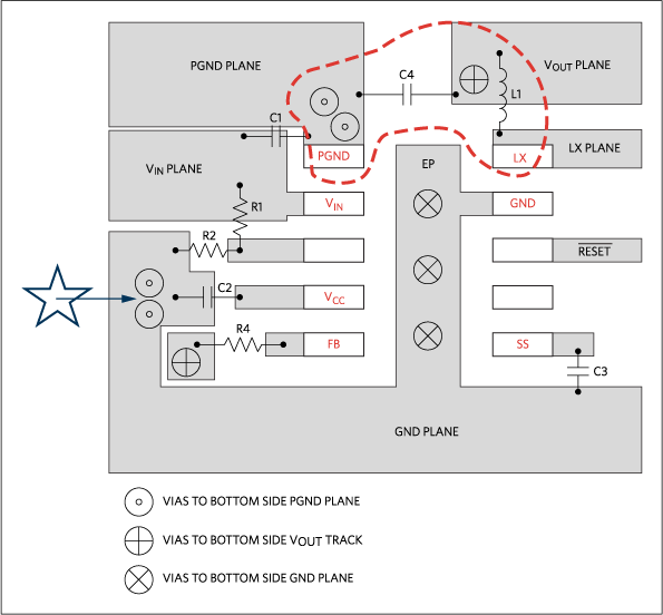 Figure 7. Isolation between grounds and ground star point and the high current loop (indicated inside the dotted red line).
The current loop of Figure 7 is the most important area of the switching power supply. Isolating the two grounds is critical for stable operation since small changes here can have devastating effects on efficiency, noise, radiated electromagnetic and radio interference. This loop contains pulsed currents, so the PCB traces must be very short and as wide as possible to reduce stray inductance. Simple changes in this current loop are the difference between a good and bad layout. By striving for the smallest loop, a bad layout will improve by 20% and become a better layout by simply rotating the inductor 90°. To reduce the series inductor inherent in a via, parallel two, four, or more vias as needed.
Looking at Figure 7, we note the via circle containing a small circle. This is the power ground plane connection (the ground triangles on the schematic) that connects to a power ground plane on the bottom side of the board and to the ground star point. The via circles containing an X are the ground for the reference and signal stability. These connect to a separate ground plane on the bottom of the board and connect to the power plane at the ground star point. The analog small-signal or reference ground and the power ground for switching currents must be kept separate. They should be connected together at a point where switching activity is at a minimum (star point), typically the return terminal of the VCC bypass capacitor.
The via circle containing the plus symbol connects the output voltage to the feedback pin. This needs to be routed away from the inductor and the power loop as quickly as possible. The series resistor (R4) must be as close as possible to the feedback pin as it, along with the input capacitance of the feedback pin, produces a lowpass filter as shown in Figure 8.
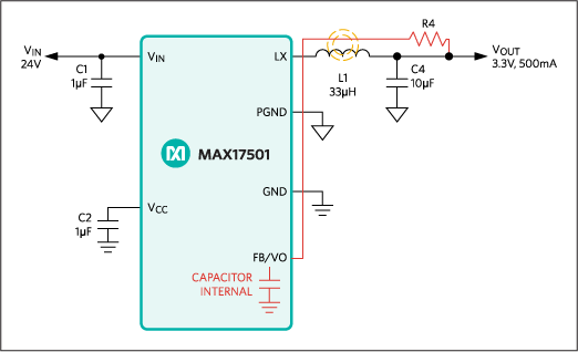 Figure 8. With R4 near the output pin, the long lead to the feedback pin (FB/VO) acts as an antenna.
An inexperienced layout person may look at the schematic and place R4 near the power output, as in Figure 8. Because the inductor is an unshielded coil of wire with a ferrite core it intensifies the electromagnetic fields that crosstalks into the feedback pin (orange dotted circles). This results in unstable operation as the wire between the feedback pin and R4 becomes an antenna, picking up the switching edges.
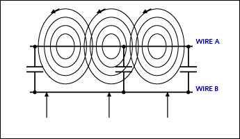 Figure 9. Crosstalk between wires may be capacitive, magnetic, electrostatic or a combination of these.
In Figure 9, wire A is the high level source and wire B is the high-impedance receiver. Crosstalk can be reduced by moving wire B away or decreasing its impedance.
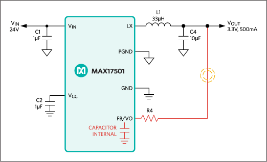
Figure 10. Proper signal routing minimizes crosstalk. The combination of R4 and “C internal” acts as a lowpass filter to reduce crosstalk.
Remember, the power switching may only run a few tens of kilohertz, however, it is the switching-edge harmonics that crosstalk and radiate. The harmonics can extend for many hundreds of megahertz and need to be controlled. This is why Figure 10 is a better way to connect the power output pin to the feedback pin. We keep the trace away from the high current loop (Figure 7) and the inductor L1. R4 will attenuate any interference shown by the orange circles. Having R4 near the MAX17501 feedback pin improves the lowpass filtering of R4 and the internal capacitance.
We have covered the simplest layout of a device that contains internal switching transistors to explain the basic concepts. Refer to other Maxim Integrated tutorials and application notes that cover devices with external transistors.6, 7, 8, 9
Conclusion
The time spent in carefully laying out the power supply will bring multiple dividends and result in an efficient quiet supply. That in turn acts as a good foundation for the rest of the circuitry by providing good clean power and ground as necessary in every circuit. Another advantage to the design engineer is that good power and ground will make the troubleshooting of other circuits relatively easy. Tracking down sporadic or intermittent errors in the presence of noisy power and ground is a real nightmare. Experienced engineers never ignore the importance of the power-supply layout by minimizing it or assigning it to the least experienced engineer. It is just that important.
References:
Maxim Integrated tutorial 3630, Power Supply and Ground Design for a WiFi Transceiver, Figures 2 and 3.
KEMET SPICE Software, Kemet®, The Capacitance Company, (Capacitor Self-Resonance) (Freeware).
www.kemet.com/Spice
Johanson Technology, JTIsoft® (freeware) is comprised of two advanced design simulation software packages, MLCsoft® and MLIsoft®. This software provides complete S-parameter and SPICE modeling data on Johanson's line of RF multilayer ceramic capacitors and inductors over the frequency range of 1MHz to 20GHz.
www.johansontechnology.com/modeling-software/jtisoftr-overview.html#.VCC3ZBYXPEc
AVX Corporation Spice Software website, www.avx.com/SpiApps/default.asp.
American Technical Ceramics, Circuit Designer’s Notebook, (Capacitor handbook). www.atceramics.com/Userfiles/cdn_nb_brochure.pdf
Maxim Integrated tutorial 2997, Basic Switching-Regulator-Layout Techniques, March 25, 2004.
Maxim Integrated application note 4944, Layout Guidelines Maximize Automotive Power-Supply Performance and Minimize Emissions.
Maxim Integrated tutorial 716, Proper Layout and Component Selection Controls EMI.
Maxim Integrated application note 3645, Correct Board Layout Lowers EMI of Switchmode Converters.
Advertisement
Learn more about Maxim Integrated


