By Nazzareno (Reno) Rossetti, Ph.D. EE, and Warren Tsai, director of business management, Maxim Integrated, www.maximintegrated.com
Advanced driver assistance systems (ADAS) are one of the fastest-growing segments in automotive electronics (Fig. 1 ). The smart car is loaded with ADAS electronic control units (ECUs), each taking power from the car battery. Each ECU supports a specific car function and has its own dedicated power management. With such a high level of variability, using a discrete approach to the ECU’s power management implementation might seem like the only option — that is, one ad hoc IC for each building block, such as in the typical system shown in Fig. 2 .
However, this approach is incompatible with another important requirement of these ubiquitous devices — specifically, small size. This article reviews three very different ECU applications and shows that even when multiple building blocks are required, a tailored integrated approach to power management can easily solve this dilemma.
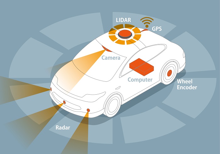
Fig. 1: Smart car loaded with ADAS sensors.
The smart car
Sensing devices in smart, autonomous, or semi-autonomous cars combine millimeter-wave radars, micrometer-wave lidars, and nanometer-wave cameras. When tracking another vehicle in front of the car, the camera is used to find and locate the preceding vehicle while the radar measures the distance. This information is then used to decide whether it is necessary to slow down or brake the vehicle. In more sophisticated systems, the distance is measured with a radar and a lidar. Unlike both lidar and radar, cameras can see color, making them the best for scene interpretation.
Today’s ADAS radar power solution
Every ADAS-compliant subsystem in the car, be it the radar, lidar, or the camera module, employs a number of voltage regulators, monitors, and watchdog ICs for proper operation. The discrete ADAS radar system in Fig. 2 shows six different ICs that implement the power management system for the monolithic microwave IC (MMIC) at the heart of the radar module.
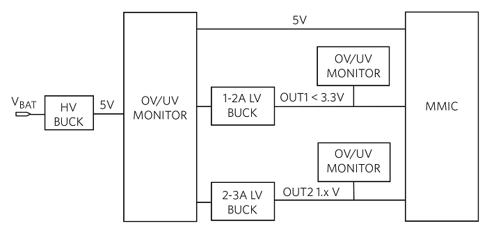
Fig. 2: Discrete ADAS radar power management ECU.
Often, the entire module must be housed on a PC board (PCB) no bigger than 50 × 50 mm, making it very challenging to accommodate all of the necessary components. A non-integrated solution like the one in Fig. 2 is space-consuming and expensive.
Another problem is that proper operation requires the battery to never discharge below 6 V (5-V output plus 1-V headroom for the high-voltage [HV] buck converter). Hence, for a cold-crank specification requiring operation down to 4 V, this scheme needs an additional pre-boost converter IC. It is estimated that the discrete implementation may require a power management total solution area of 1,250 mm2 , or half of the available space.
On the other hand, a single power management IC would subject all the blocks to the battery voltage variability. Furthermore, an excessive level of integration may create a monster PMIC that is too big to place in the available niches of the square PCB, where the lion’s share of the space is taken up by the signal chain. It is, indeed, crucial to make the right decision on integration partitioning.
Ideal ADAS radar power solution
An ideal solution should operate with an input voltage at the lowest battery voltage while withstanding load “dump.” Fig. 3 shows six chips in Fig. 2 that are reduced to two. The HV buck converter withstands the load dump and takes the battery voltage down to 3.3 V, allowing for cold-crank operation near its output (well below 6 V). A high-density, low-voltage PMIC integrates the back-end voltage regulators. With this partitioning, the required area can be conveniently split into two chunks, one for the front-end buck converter (HV BUCK) and one for the PMIC, making it easy to “wrap” the power management solution around the signal chain circuitry.
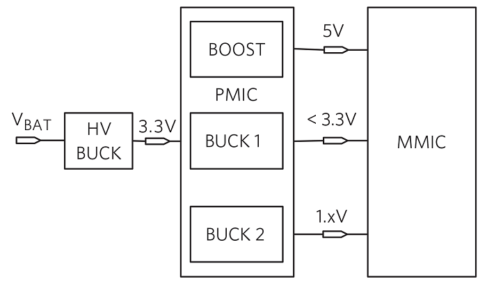
Fig. 3: ADAS radar PMIC.
A small PMIC that fits this type of ADAS radar application is the MAX20014 , which provides three high-efficiency, low-voltage DC/DC converter outputs. VOUT1 boosts the input supply up to 8.5 V at up to 500 mA, while two synchronous step-down converters operate from a 3.0-V to 5.5-V input voltage range and provide a 0.8-V to 3.8-V output voltage range up to 3 A.
An HV BUCK, such as the MAX20075 (600 mA/1.2 A), interfaces with the battery. A 2.5-A version of that device (MAX20077) is also available.
In this implementation, the ADAS radar power management total solution area is estimated to be 750 mm2 , or about one-third of the available area (versus half for the non-integrated solution). Additional pin-compatible versions of the IC can support different system requirements.
Ideal ADAS camera power solution
The previous partitioning solution can be replicated for an automotive camera ECU. Fig. 4 shows the PMIC inside the ECU, comprised of only an 8.5-V boost converter and a 1.8-V buck converter. The 1.8-V rail powers the microprocessor. The 8.5-V rail is routed through coaxial cables to power the remote cameras.
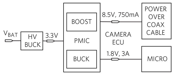 Fig. 4: Power PMIC inside the camera ECU.
A PMIC tailored for ADAS camera ECU applications is the MAX20414 , which integrates one sync boost and one step-down converter. The total solution area (PMIC + HV BUCK) is estimated to be about 550 mm2 .
Ideal instrument cluster ECU power solution
The instrument cluster MCU processes the information displayed by the dashboard instrumentation. In Fig. 5 , the SoC microcontroller needs two power sources, 1.1 V to power its core and 1.8 V for the periphery. Here, a dual-buck PMIC like the MAX20416 , which has a dual-output, low-voltage step-down converter, fits the ADAS microprocessor core and periphery power supply application. The total solution area (PMIC + HV BUCK) is estimated to be about 560 mm2 .
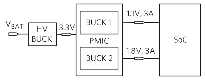 Fig. 5: Instrument cluster PMIC.
In each case, the level of PMIC integration needed to fit the solution into a small available space, along with a load-dump tolerant, high-voltage front-end buck converter, is achieved with a tailored approach. This leads to efficiency in terms of cost as well as PCB area.
Additional requirements that these ICs must meet for ADAS applications include: compliance to automotive standards, the ability to operate at high frequency to avoid AM radio-band noise interference, output voltages with ±1.5% accuracy to meet SoC power supply requirements, spread spectrum for low EMI emissions, and integrated overvoltage and undervoltage monitoring features.
Conclusion
We reviewed three very different automotive ADAS ECU applications. In each case, a tailored approach to integration was proposed. Each system was partitioned into a high-voltage front-end IC and a low-voltage back-end PMIC. The entire power management system was reduced to two ICs, a level of complexity that is small enough to fit into the limited board space required by ADAS applications, by “wrapping” it around the signal chain circuitry.
About the authors
Warren Tsai is a director of business management at Maxim Integrated. He holds both a Bachelor of Science degree in electrial engineering and computer science and an MBA from UC-Berkeley. He has held various design engineering, applications engineering, and product management responsibilities in his career, and his team manages all of Maxim’s automotive power solutions.
Advertisement
Learn more about Electronic Products MagazineMaxim Integrated


