By Arash Loloee, Senior IC Design Engineer and Member Group Technical Staff, Texas Instruments
It is not surprising that the world around us is getting more and more digitized. One reason might be that manipulation, storage, and usage of data in digital form is more convenient and easier than analog form. That puts more importance on circuits that convert the analog signals into digital forms for further processing and use.
When using an analog-to-digital converter (ADC) in any circuit, the user’s first inquiry is the number of bits (NOB), followed by the sampling rate. But it is the effective number of bits (ENOB) that will tell you a great deal about the converter itself. Along with ENOB, the sampling frequency, spurious-free dynamic range (SFDR), integral nonlinearity (INL), and differential nonlinearity (DNL) are among the parameters that can guide you when selecting a prospective ADC.
In this article, I’ll discuss the effect of various parameters on dynamic behavior, including those that have the most prominent effect on signal-to-noise ratio (SNR), along with some static behavior of ADCs. I will start by examining the effects of several key parameters on the SNR, such as jitter, quantization noise, input signal, and DNL.
Jitter
The uncertainty in the sampling clock results in an error in the sampled voltage, as shown in Fig. 1 , which depicts the error in sampling voltage caused by clock jitter.
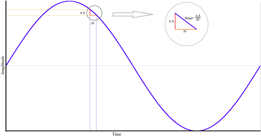
Fig. 1: Sampling clock jitter.
Consider an input signal of the form of Vin = Vp sin (2pfin ). The derivative of the input signal with respect to time is the rate of its change. The maximum change occurs when the cos(2pfin ) is equal to 1, resulting in Equation 1:

To ensure that the voltage error from jitter (tj ) is tolerable for a given N-bit ADC with a full-scale voltage (VFS), it has to be smaller than VLSB /2 (Equation 2), wherein VLSB is defined by VFS/2N :
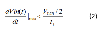
For the given sine wave in Equation 1, you can solve for jitter (tj) using Equation 3:

I used Vp-p = VFS and Vp = 2N–1 VLSB to rewrite the equation.
For a 12-bit ADC with an input frequency of 80 MHz, the jitter must be smaller than 485 ps not to cause a sampling error.
Now let’s look into the theoretical effect of jitter on the SNR of the ADC. If Ve-RMS is the worst-case root-mean-square (RMS) voltage error for tj for the input sine wave, Equation 4 is:

Equation 5 expresses the contribution of jitter error to SNR as:

Quantization noise
Because ADCs represent a distinct range of analog inputs for a given code, there is bound to be an error associated with each digital code. Simply put, although a range of analog inputs is assigned to a given code, only one analog input is represented accurately for the given code. As a result, there is an error associated for the assigned code to a given analog input. This error can range from –LSB/2 to +LSB/2.
As an example, in Fig. 2 , all analog inputs in the range of 2.5 to 3.5 are represented with the same digital code: 0 … 011.
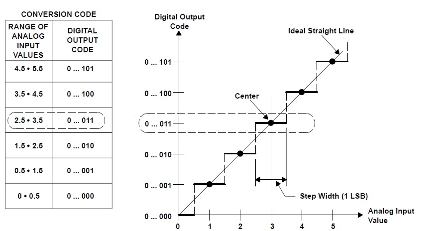
Fig. 2: Ideal transfer function of an ADC.
Each input in this range has an error that is bigger at the boundary of the range (with different polarity); the error gets smaller as you get closer to the center of the range. Plotting the quantization error versus the analog input range results in the well-known sawtooth plot, as shown in Fig. 3 .
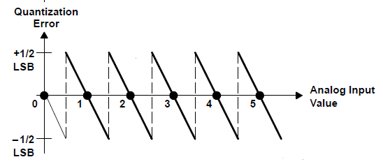
Fig. 3: Inherent quantization error.
Equation 6 calculates the average noise power (mean square) of the error over a step, wherein q is equal to 1 LSB:

Therefore, Equation 7 gives the SNR power ratio as:

If you include quantization noise and overall noise — the composite RMS DNL — along with input noise to the jitter effect described in Equation 5, you would get Equation 8:

The first term inside the bracket is the effect of jitter discussed earlier. The second term is the effect of quantization noise and linearity error, and the third term is the effect of input noise.
In an ideal case in which jitter, quantization noise, and input noise are zero, you’ll get the following well-known equation for SNR (Equation 9):

In practice, usually, the first two terms of Equation 8 are used and the third term is ignored. You can use Equation 8 to calculate jitter and quantization error from measured SNR under specific conditions. To calculate the quantization error, a low fin is applied whereby the effect of jitter is negligible and can be neglected. You can use the measurement of the resulting low-frequency SNR to calculate ε in Equation 10:

To calculate jitter, a high-frequency input is applied and SNR is measured again. In this case, jitter is the main contributor to the degradation of SNR. Using the new SNR at the high frequency of f , you can readily calculate tj with Equation 11:

Input signal
If the input is not full-scale, it will degrade the SNR accordingly, an effect that is easily quantifiable. For example, if the input sine wave has an amplitude of Vin , which is a fraction of full scale, then the ideal SNR will be reduced by 20 log (2Vin /VFS ). If a sine wave with a 2-V amplitude is applied to a 12-bit ADC with a VFS of 5 V, the input will reduce the theoretical SNR of 74 dB by 1.938 dB and result in an SNR of 72.062 dB.
Another dynamic performance parameter for an ADC is the signal-to-noise and distortion ratio (SINAD or SNRD). SINAD is related to ENOB in the same way that SNR and NOB are related. By definition, you can calculate SINAD by including the noise and total harmonic distortion (THD) effect (Equation 12):

Alternatively, you can express SINAD in terms of ENOB simply by using Equation 10 and replacing SNR for SINAD and N for ENOB.
Oversampling
So far, I have assumed sampling at the Nyquist rate, meaning that the sampling rate is twice the maximum frequency of the signal being sampled. Now, let’s study the effect of oversampling — sampling beyond the Nyquist rate — on SNR. For this purpose, the ratio of sampling frequency (fos) to the Nyquist frequency, 2 fo, is the oversampling rate (OSR = fos /2f0 ).
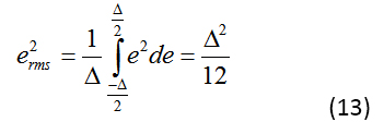
But first, let’s look at the quantization error, ε, used in previous equations to calculate SNR. ε has an equal probability of lying between ±(Δ/2), wherein D is the LSB or simply VFS /2N . Equation 13 expresses the quantization noise power as:
Equation 14 gives the noise power that falls into the signal bandwidth (0 to fo) as:

Equation 14 illustrates an interesting point: Oversampling decreases quantization noise in the band of interest, which results in improved SNR. In fact, you can quantify the improvement in SNR using Equation 15:

From Equation 15, you can see that SNR improves by 3 dB per octave. So, if OSR = 2, then the SNR improves by 3 dB; if OSR = 4, the SNR improves by 6 dB.
In Fig. 4 , the sampling frequency has increased by 3 dB per octave; thus, the noise floor has dropped by 9 dB, which is equivalent to improved SNR by the same amount.
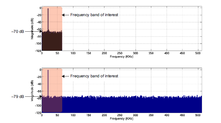
Fig. 4: Reduction of noise floor due to oversampling.
DNL
DNL errors reduce overall SNR. Below a certain frequency, THD is only dependent on the overall INL of the ADC; beyond that frequency, the dynamic performance of the converter comes into the picture.
Let’s formulate the limit of 1 LSB DNL, which is the condition for not having a missing code; this is equivalent to a 1-bit reduction in resolution and, thus, a reduction of SNR by 6 dB. For an n-bit converter with a 1 LSB linearity error, Equation 16 expresses the SNR boundary due to linearity error as:

This is a first-order approximation. Although valid only when there is no missing code, Equation 17 gives the SNR degradation caused by DNL as:

Summary
Clock jitter, sampling rate, and quantization noise are the most critical factors affecting the SNR and SFDR in ADCs. Factors like jitter and sampling rate can affect the expected and theoretical values of many important parameters such as SNR. By understanding the factors affecting SNR and utilizing some method to quantify the effect, one can better estimate the SNR for a given ADC. Additionally, we can try to optimize the design to obtain the target specifications after understanding and quantifying those factors’ effects on performance.
About the author
Arash Loloee is a senior integrated-circuit design engineer and Member Group Technical Staff at Texas Instruments. His responsibilities include designing and modeling transistor- to system-level projects. He was a lecturer from 2005 to 2010 at the University of Texas at Dallas, where he taught various analog and digital courses. He has a bachelor’s degree in physics from the University of North Texas and master’s and Ph.D. degrees in electrical engineering from Southern Methodist University. For questions about this article, please contact Arash at .
References
- “Understanding Data Converters.” Texas Instruments application report SLAA013: 1995.
- Brown, Ryan, and Sameer Singh. “General Oversampling of MSP ADCs for Higher Resolution.” Texas Instruments application report SLAA694A: 2016.
- Jenq, Y.C., and Qiong Li. “Differential Non-Linearity, Integral Non-Linearity and Signal to Noise Ratio of an Analog to Digital Converter.” Department of Electrical and Computer Engineering, Portland State University.
- Duan, Jingbo, Le Jin, and Degang Chen. “INL Based Dynamic Performance Estimation for ADC BIST.” Proceedings of the 2010 IEEE International Symposium on Circuits and Systems (ISCAS), May 30–June 2, 2010.
- Opris, Ion E. “Challenges in A/D Design and Practical Understanding of A/D Specifications.” IEEE Chapter Meeting Presentation, April 17, 2003.
- Xu, Fang. “A New Approach for the Nonlinearity Test of ADCs/DACs and Its Application for BIST.” European Test Workshop 1999 Proceedings: 34–39.
- Lin, Chun Wei, and Shih Chung Luo. “Estimating Total-Harmonic-Distortion of Analog Signal in Time-Domain.” 2012 18th International Mixed-Signals, Sensors and Systems Test Workshop, May 14–16, 2012.
Advertisement
Learn more about Electronic Products Magazine


