Finding the right architecture for your design
BY KEVIN TRETTER
Microchip Technology
Chandler, AZ
www.microchip.com
As technological advances continue to drive down the prices of ICs, more and more system designers are opting for higher-precision operational amplifiers. These devices can simplify system design and/or manufacturing by eliminating the need for a system calibration, either during manufacturing or while the product is in the field. However, today’s system designer has many options when it comes to low-offset op amps. Multiple architectures exist, including the use of nonvolatile memory, laser trimming, auto-zeroing and even on-chip calibration circuitry. This article will explain the fundamentals of these various architectures, and explore the benefits and shortcomings of each.
Precision op amps
Before discussing the various op-amp architectures, it is important to clarify what is meant by the term “precision” op amp. This term typically relates to the input offset voltage of the amplifier. As the name implies, this specification is the amplifier’s voltage difference between the inverting and non-inverting inputs. This error voltage can vary from microvolts up to millivolts, and is highly dependent on how well matched the input transistors are. A “precision” amplifier implements some form of input offset correction, typically by using one of the architectures discussed here.
When discussing precision op amps, it is important to not only consider the initial input offset voltage, but also the behavior of this error voltage across various environmental conditions. These environmental conditions include changes in common-mode voltage, operating voltage, output voltage, temperature, and even time. Depending on the application, these external conditions may determine the best amplifier architecture for your design.
Nonvolatile memory (NVM)
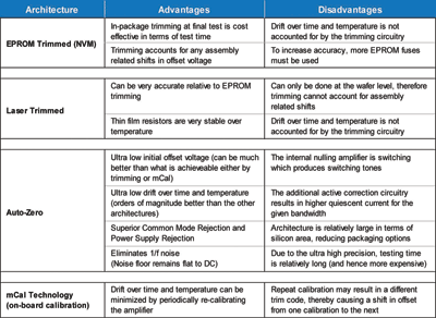
The first architecture uses nonvolatile memory. This method implements nonvolatile EPROM fuses to correct the input offset voltage of the amplifier. In many cases, this process is done in-package during the final test of the device, and is a very cost-effective way to provide an amplifier with low initial offset voltage.
Since the trimming is done post-assembly, any assembly-related offsets can be corrected. The other advantage of this architecture is that it does not require any customer inputs. The amplifier is trimmed by the manufacturer and does not require the customer to do anything.
However, the EPROM fuses take up a certain amount of silicon area. Hence, the EPROM-trimmed devices can be somewhat limited in terms of ultra-small packaging. Also, like a general-purpose amplifier, this architecture will be sensitive to environmental conditions such as temperature, as well as changes in common mode or operating voltage.
Laser trimming
Another method often used to increase the accuracy of an op amp is laser trimming. This process involves using a laser to adjust the resistance value of thin-film resistors located within the silicon wafer. The accuracy of this approach can be relatively high, since the trimming process is continuous (as opposed to involving discrete steps, as in EPROM trimming). Another advantage of laser trimming thin-film resistors is that these resistors are inherently very stable over temperature, adding to the overall accuracy of the amplifier across a wide temperature range.
However, laser trimming cannot be done within a packaged device, and can only happen at the wafer level. The processes of sawing the wafer into individual die, placing the die in a package, and bonding the die to the packaged pins can all cause mechanical stress on the wafer that will negatively affect the overall accuracy of the device. Such assembly-related changes cannot be accounted for when trimming and, hence, will add to the error of the amplifier.
Like non-volatile memory fuses, laser trimming is done once during the time of manufacture, with no option to retrim the device. Therefore, changes in external operating conditions will adversely affect the accuracy of the amplifier. The voltage offset error of the amplifier across these external conditions (such as temperature, operating voltage, etc.) must be carefully considered, as this behavior could directly impact the performance of the overall design.
Auto-zero architecture
The auto-zero architecture is a continuously self-correcting architecture that uses a null amplifier to correct the offset voltage of the main amplifier. This architecture enables ultra-low offset error (can be 100 times better then an EPROM trimmed amplifier, for example), and low offset drift, and eliminates 1/f noise while providing superior power-supply and common-mode rejection.
Since this architecture is continuously self-correcting the input offset voltage, it is inherently insensitive to the environment. Changes over temperature and aging, as well as changes in operating voltage or common-mode voltage, will have very little effect on the accuracy of the auto-zero amplifier.
Finally, the self-correcting circuitry is all contained on-chip, so no customer input is required. From the system-level point of view, the device looks and functions just like a standard op amp, only with exceptional performance. Figure 1 shows an example auto-zero op amp.
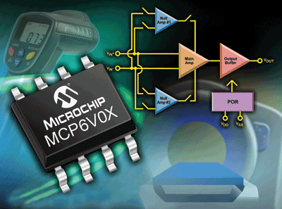
Fig. 1. Op amps such as the MCP6V0X have an auto-zero architecture.
Despite all of these advantages, the self-correcting auto zero architecture does have its downside. The internal correction circuitry is continuously switching, which produces switching noise. This additional circuitry also results in a higher quiescent current for the given bandwidth. Finally, due to the ultra-high precision of this type of device, testing time can be relatively long, resulting in a more expensive device to manufacture.
On-chip calibration circuitry
Microchip’s mCal technology provides yet another means of enabling high-precision op amps. The technology involves an on-chip calibration circuit. Much like the other methods discussed, this calibration results in very low initial offset voltages. However, unlike EPROM or laser-trimmed amplifiers, the on-chip calibration circuitry is active upon power up, or based on an external calibration pin. This enables the user to recalibrate the amplifier as often as they like. By recalibrating the amplifier somewhat frequently, the accuracy of the amplifier can become somewhat insensitive to the environment.
For example, if a customer is very concerned about drift over temperature, they can minimize drift error by recalibrating the device every time the temperature changes by 5. Although this can significantly reduce the drift of the amplifier over temperature, this recalibration technique requires the user to actively initiate a calibration routine by toggling the calibration pin on the amplifier.
Today’s system designer has many choices when it comes to selecting an op amp for his or her design. Most applications can benefit from the use of a higher-precision op amp, but it is critical that the designer understand the underlying architecture of the amplifier.
Although all of the methods discussed in this article will provide an amplifier with low initial offset voltage, the accuracy of the amplifier can vary significantly due to environmental conditions. The use of a continuously self-correcting architecture, such as an auto-zero amplifier or an amplifier with the ability to recalibrate using mCal provides a means to counter the adverse effects of external conditions. Table 1 provides a summary of these four different architectures. ■
Advertisement
Learn more about Microchip Technology


