What you need to know to configure an unused op amp in a quad or dual op-amp device
BY TODD TOPORSKI
Analog Applications Engineer
Texas Instruments
www.ti.com
A common question among customers is, “How should I configure an unused operational amplifier (op amp) in my quad or dual op-amp device?” While this may seem like a simple question, there are subtle aspects of operational amplifier behavior that must be understood to arrive at the correct implementation. Once you understand the basics and avoid all possible problem scenarios, a properly terminated op-amp circuit can be achieved.
Avoiding adverse conditions
There are several possible conditions to which an unused op-amp stage can be subjected, if left unconnected or improperly terminated. These include: (1) susceptibility to noise; (2) extra power consumption; (3) extra power dissipation; and (4) electrical overstress (EOS). All these conditions can lead to device degradation and possible failure.
Also consider that one stage (unused or not) behaving in an adverse or unexpected manner also can impact the performance of the other op-amp stages in the same device. Even if device failure is not likely or does not occur, performance degradation in the other stages is still of concern.
Main op amp considerations
Inputs, output, and gain must be carefully considered for any op amp, whether used in an intended circuit or left unused.
1. Inputs: The input stage is complex and has several important specifications:
a. Input common-mode range: Must be met to prevent unexpected non-linear output behavior, including saturation and phase inversion. Exceeding the supply rail can expose the device to a latch-up condition. Latch-up can occur when current biases on diodes and transistors in an unexpected manner, and can result in short circuiting the supply rails and possible device failure.
b. Differential input voltage rating: Exceeding this maximum voltage rating between inputs can overstress the input stage and cause op-amp failure.
c. Input offset voltage (V IO ): A small differential voltage between the inputs, which can be amplified and impact output performance.
2. Output: The output stage can saturate (or rail out) when it is driven near either supply rail. A saturated op amp consumes more supply current and dissipates more power than one that is not saturated.
3. Gain/Feedback: Op amps have very large open-loop gain. Gain should be limited to something relatively small that prevents noise from being amplified and the output from saturating. Negative feedback is recommended to set gain and achieve stable, predictable behavior.
Common implementations
In practice a number of circuits are commonly implemented or considered by system designers having spare op amps. Using parameters and considerations discussed, let’s examine each of these circuits and predict possible behavior.

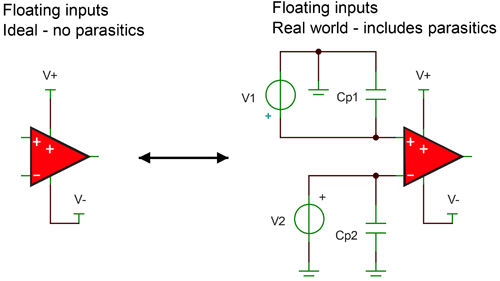
Fig. 1: Floating op-amp inputs are subject to parasitic capacitances and nearby electric fields.
In Fig. 1, both inputs and outputs are left unconnected or floating. Ideally, there are no parasitic circuits on the printed circuit board (PCB). But in reality, stray capacitances exist that can couple the inputs to ground (GND) or other voltage potentials. Depending on your PCB design, voltage levels, cable routing, and a number of other factors, it is possible for a stray electric field to couple to either or both input pins.
If electric fields V1 and V2 contain voltages larger than the specified input range of the op amp, then the input common-mode range is violated. If V1 or V2 also exceed the supply rail, latch-up or electrical overstress (EOS) may occur. Inputs left floating are also susceptible to electromagnetic interference (EMI) or radio frequency interference (RFI). Clearly, this implementation should be avoided due to potential failure.
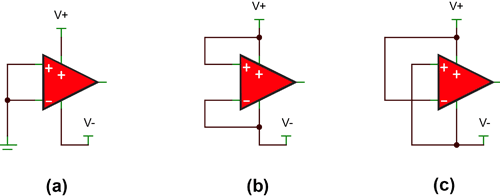
What about connecting the inputs to GND or the supply rails, either directly or through resistors? Figure 2 shows three implementations, which initially appear to be an improvement over Fig. 1. The inputs no longer float and are not as susceptible to stray electric fields or EMI/RFI. Upon closer inspection we can identify other potential issues.

Fig. 2: Op amps with (a) both inputs connected to ground, or (b and c) inputs connected to separate supply rails, should be avoided.
The circuit in Fig. 2a connects both inputs together and to GND, but it ignores the effects of input offset voltage (VIO ) between the inputs. Depending on the polarity of VIO , the small voltage between the inputs causes the output to drive to one supply rail or the other. Since this circuit has large open loop gain, the output saturates and the device consumes extra current. This implementation should be avoided.
The circuits in Figs. 2b and 2c connect the inputs to opposite supply rails. VIO won’t be a problem, but there are pitfalls to this approach. It assumes the specified input range can accommodate the inputs being connected in this manner. Many op amps cannot accommodate a differential input voltage from supply rail to supply rail. In these cases the input stage can suffer EOS and damage. These circuits also lack feedback and exhibit high open loop gain, such that output of 2b can saturate to the V+ rail and 2c can saturate to the V– rail. Also avoid these implementations.
Proper termination
After carefully considering op-amp parameters and limitations, proper termination can be achieved. Make sure the inputs meet all input requirements, including input common-mode range and maximum differential input voltage rating. Do not connect the inputs together. Add negative feedback for stability, and place the output at a voltage level that prevents the op amp from saturating.

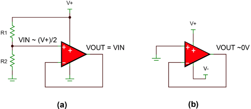
Fig. 3: Properly terminating an op amp powered from (a) single supply rail or (b) split supplies.
Figure 3 describes a circuit that addresses the basic requirements and concerns previously discussed. A very simple unity-gain voltage follower can be used to meet all criteria. In the single supply case in Fig. 3a, a voltage VIN is set by R-divider R1 and R2 and applied to the non-inverting input. Choose the level of VIN to meet the input common-mode voltage range specified in the datasheet. For most op amps, placing VIN midway between the supply rails works fine and is easy to implement using a divide-by-two R-divider. Since the circuit is unity gain and has negative feedback (output to inverting input), it remains stable and does not amplify the input. The output is approximately VIN and output saturation is avoided.
For the case of a split (dual-polarity) supply in Fig. 3b, it is assumed that GND (0 V) is the midpoint between the two supply rails. The termination circuit is further simplified in this case since the non-inverting input can be directly connected to GND. In both implementations the termination circuit minimizes supply current consumption and power dissipation, and improves immunity to noise and other problems at the inputs. For any provided supply rails, Fig. 3 shows the proper method to terminate an unused op amp! ■
Reference
Diagrams in this article were created using TINA-TI SPICE: www.ti.com/tool/tina-ti.
About the author
Todd Toporski is a Member of Group Technical Staff at Texas Instruments where he specializes in analog applications. Todd received his BSEE degree from Michigan Technological University and his MSEE degree from The Georgia Institute of Technology. Todd can be reached at
Related Products: Standard and Specialty Logic
Advertisement
Learn more about Texas Instruments


