Renesas Electronics Corp. recently announced the development of two 2.4-GHz RF transceiver technologies for IoT devices that support the Bluetooth Low Energy (LE) low-power, near-field communication standard. With the new matching circuit and signal correction technologies, Renesas designed a prototype circuit, which it claims is the smallest Bluetooth LE RF transceiver, while boosting power efficiency.
Renesas developed the technologies to help companies with increasing requirements for RF expertise in the IoT space. “The increase of IoT applications requires RF functions by engineers who are not experts in RF technology compared to smartphone and PC engineers,” said Hisayasu Sato, Ph.D., senior principal engineer, Connectivity & Audio Business Division, Renesas. “BLE needs to be easy to use for many engineers who are not RF experts.”
The new matching circuit technology covers a wide impedance range and enables the IC to match a variety of antenna and board impedances without an external impedance-matching circuit. The new signal correction technology for locally generated reference signals uses a small circuit to self-correct inconsistencies in the circuit elements and variations in surrounding conditions without calibration, said Renesas.
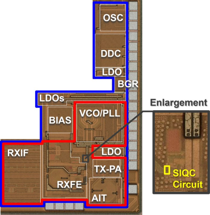
The company has verified these technologies on a Bluetooth LE RF transceiver circuit prototype built on a 22-nm CMOS process. The prototype showcases a reduced circuit area including the power supply, measuring 0.84 mm2. The small size was achieved by modifying the receiver architecture to reduce the number of inductors and making enhancements such as a low-current baseband amplifier with a small mounting area and a highly efficient class-D amplifier.
In addition, Renesas claims best-in-class power efficiency, with power consumption of 3.6 mW and 4.1 mW during reception and transmission, respectively. For designers, these advances could translate into a smaller size, reduced board cost, lower power consumption, and a simpler board design process.

The reference signal self-correction circuit technology eliminates the need for a calibration circuit. Click for a larger image. (Source: Renesas Electronics)
Matching circuit technology covers wide impedance range
About six years ago, Renesas presented an integrated impedance-matching circuit technology that enabled the design of compact and low-cost Bluetooth LE products that required no external inductors or capacitors for switching between reception and transmission or impedance matching.
But the impedance did not necessarily reach 50 Ω, depending on the antenna or board design, and an external matching circuit was still needed, said Renesas. Also, when using the earlier technology and adding the matching circuit with impedance-changing functionality, other issues could arise, including increased signal loss and the inability to achieve a sufficient range of variation, said the company.
To solve these challenges, Renesas has developed a new variable impedance-matching circuit technology, consisting of two inductors and four variable capacitors. In this new design, the transmitter-side inductor and receiver-side inductor used in the matching circuit are configured in a concentric arrangement, and their mutual induction is used to reduce signal loss and cut the effective parasitic capacitance, said Renesas.
The result is an expanded variable impedance range and a smaller circuit area. Renesas confirmed a voltage standing wave ratio (VSWR) of 6.8 maximum and a variable impedance range of approximately 25 to 300 Ω.
Reference signal self-correction circuit technology eliminates calibration circuit
A reference signal of about the same frequency as that of the wireless radio signals received via an antenna is generated internally by the RF transceiver, and this signal is used to convert gigahertz-band wireless signals to low-frequency baseband signals, said Renesas. The challenge is the reference signal accuracy can be degraded by factors such as inconsistencies in the circuit elements or variations in the temperature or supply voltage, said the company.
Compensation technology has been used for phase and amplitude deviations with a calibration circuit to accurately generate the reference signal. But there were a couple of challenges. Integrating a calibration circuit required a larger chip area, higher power consumption, and increased test cost, said Renesas.
These challenges were solved with Renesas’s new self-IQ-phase correction circuit technology that uses reference signals of four different phases to correct each other by allowing the phase differences to cancel each other out. Renesas said the “image signal rejection ratio, critical for reception performance, averages 39 dB, which meets the Bluetooth standard with a comfortable margin to spare.”
In addition, the self-correction circuit can be implemented at approximately one-twelfth the size of a conventional calibration circuit. And it also delivers power consumption and cost benefits, said Renesas.
These technologies can be used for different types of RF transceivers in addition to Bluetooth LE. “Since it is not a technology limited to BLE, applications such as Wi-Fi and sub-GHz, are assumed, but we will continue to study further in the future to determine whether it is actually applicable. These technologies contribute to low cost and low power for those wireless applications,” said Sato.
Renesas is currently working on practical applications for these technologies. Sato said the company just now is beginning to consider using these technologies for its MCUs and wireless products. Target launch dates have not been set.
Advertisement
Learn more about Renesas Electronics America


