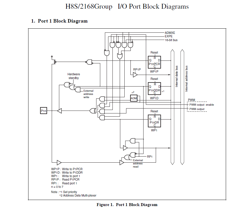
This LSI is a microcomputer (MCU) made up of the H8S/2000 CPU with Renesas Electronics's exclusive architecture as its core, and the peripheral functions required to configure a system such as PC server.
The H8S/2000 CPU has an internal 32-bit configuration, sixteen 16-bit general registers, and a simple and optimized instruction set for high-speed operation.The H8S/2000 CPU can handle a 16-Mbyte linear address space. The instruction set of the H8S/2000 CPU maintains upward compatibility at the object level with the H8/300 and H8/300H CPUs. This allows a transition from the H8/300, H8/300L,or H8/300H to the H8S/2000 CPU.
This LSI is equipped with ROM, RAM, two kinds of PWM timers (PWM and PWMX), a16-bit free running timer (FRT), an 8-bit timer (TMR), a watchdog timer (WDT),a serial communication interface (SCI), an I 2 C bus interface(IIC), an LPC interface (LPC), a D/A converter, an A/D converter, and I/O ports as on-chip peripheral modules required for system configuration.
A data transfer controller (DTC) is included as a bus master.
A flash memory version is available,providing the LSI with 256, 384, or512-k bytes of ROM. The CPU and ROM are connected to a 16-bit bus,enabling byte data and word data to be accessed in a single state. This improves the instruction fetch and processing speeds.
Two operating modes are provided, offering a choice of address space and single chip mode/external extended mode. Boot programming into flash memory, on-chip emulation, and boundary scan can be selected as special operating modes.
Download Full Block Diagram Below
Advertisement

Learn more about Renesas Electronics America


