Understanding how individual components contribute to the overall performance
BY EAMON NASH, Applications Manager, RF Group
Analog Devices, Norwood, MA
www.analog.com
Every wireless signal chain design begins with signal chain choices. Once a systems engineer has decided on a signal chain architecture (e.g., superheterodyne, zero IF, IF sampling, etc.), components must be selected. In a discrete device, it is critical to select components with comparable specifications. When choosing, it’s not as simple as picking devices that have some minimum level of performance. The effect of a device’s noise and distortion on the overall signal chain is a strong function of its gain and location in the signal chain. For example, the noise of a first-stage low-noise amplifier will strongly impact the overall noise figure, whereas the noise of an Intermediate Frequency amplifier will have less of an impact.
To understand how individual components contribute to overall performance, systems engineers use the four classic equations shown in Fig. 1 , represented here for a three-stage signal chain.
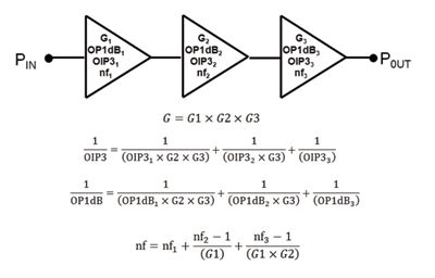
Fig. 1: Cascaded noise factor, IP3, gain, and P1dB equations for a three-stage wireless signal chain.
Gain can be easily calculated in the linear domain by multiplying the individual gains or in the log domain by summing the dB gains together. However, composite third-order intercept (IP3), 1 dB Compression (P1dB) and noise figure must be calculated in the linear domain by converting P1dB and IP3 to watts (from dBm) and by converting noise figure to noise factor (Noise figure = 10log(noise factor)).
System engineers traditionally use home-grown spreadsheets or RF simulation tools to perform these calculations. One notable limitation of these equations is that they assume a perfectly matched signal chain with no impedance discontinuities between components. In real-world systems, interstage impedance mismatches are not uncommon, and in some cases there is deliberate interstage mismatch.
As an example, Fig. 2 shows a screen shot of ADIsimRF, an RF signal chain calculator that is available free from Analog Devices. At its core, this tool implements the cascaded equations for gain, noise figure, IP3, and P1dB shown in Fig. 1 along with power consumption. The number of stages can be dynamically varied up to a maximum of 15. Additional stages can be inserted at any point in the signal chain and individual stages can be deleted or temporarily disabled.
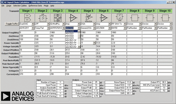
Fig. 2: Using ADIsimRF to level plan a zero-IF discrete transmitter.
ADIsimRF includes an embedded database of ADI’s discrete RF components. This database, which also includes models for passive components such as baluns and SAW filters, can be easily accessed using pull-down menus as shown in Fig. 2 . Device data (IP3, P1dB, gain, and noise figure) are stored in the database at various frequency increments. When a particular frequency is selected, the calculator uses the closest frequency datapoint in the database. Data from the internal database can be overwritten on the calculator’s front panel and custom devices can be created and saved.
Performing level planning on components that are not simple 50-Ω, two-port devices can be challenging. For example, an IQ modulator has three inputs:, I, Q, and LO. This raises the question of how to define its gain. In addition, the I and Q inputs typically have high input resistance, which suggests a very high power gain.
An IQ modulator is generally driven by a dual DAC with a Nyquist filter between the two. This filter is terminated with two shunt resistors at the I and Q inputs. These resistors are typically between 100 and 1,000 Ω, with the size of the resistor scaling the DAC voltage up or down. In order to give the IQ modulator an effective power gain, ADIsimRF considers these resistors to be part of the IQ modulator. As a result, IQ modulator gain in ADIsimRF is defined as the difference between the power delivered to each shunt resistor and the RF output power. In the case of some IQ modulators, multiple models with different input resistances are provided in the ADIsimRF database. With an output resistance of 50 Ω and an input terminating resistance that ranges from 100 to 1,000 Ω, the power gain and the voltage gain of the IQ modulator will be different.
Defining the noise figure of an IQ modulator is also not obvious. If we define the power gain of the IQ modulator as above, then the noise figure can be defined as the difference between thermal noise (–173.8 dBm/Hz) and the output noise of the IQ modulator minus the power gain. So the noise figure of an IQ modulator with a noise floor of –158 dBm/Hz and power gain of 3 dB is equal to 13 dB (i.e., –158.2 dBm/Hz = –173.8 + 3 + 13).
Modeling mixed-signal components such as A/D and D/A converters in a typical RF signal chain calculator is even more challenging. This is because a DAC does not have an obvious “gain” and because the noise and distortion of a DAC change with sampling rate, data interpolation rate, and dBFS drive level.
In the ADIsimRF tool, the “gain” of a DAC is defined as 0 dB for a 0 dBFS drive level when the output is at baseband, that is, centered at 0 Hz. When a lower dBFS level (e.g., –6 dBFS) is chosen, the gain will be lower by that amount. Also, as the DAC’s output frequency increases, the gain will decrease as the DAC output follows its sin(x)/x function.
To accommodate different DAC configurations, the ADIsimRF database includes a number of “versions” for each DAC (e.g., AD9122V1, AD9122V2, etc). Each version corresponds to different operating configurations, which include various dBFS drive levels, sample rates, and interpolation rates.
The dual, differential, high-speed DACs that are used to drive IQ modulators are generally terminated with four 50-Ω resistors to ground. The DAC’s output current flows through these resistors along with the input shunt resistance at the IQ modulator inputs. In ADIsimRF, the output power level of the DAC is the power that is delivered into the shunt resistors at the IQ modulator.
Figure 3 shows a screen shot of a level plan for a 2.5-GHz IF sampling receiver. In this receiver, the input signal is amplified and mixed down to 140 MHz before being under-sampled by an ADC. The IF stage includes the AD8375 ADC driver, whose gain can be set in 1-dB increments from –4 to +20 dB. A pull-down menu can be used to choose any of the 25 available gains as shown in Fig. 3.
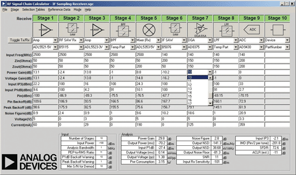
Fig. 3: Shown above is a screen shot of a level plan for a 2.5-GHz IF sampling receiver.
Like DACs, fitting an ADC into a RF signal chain calculator is not trivial. One common problem stems from the fact that the input impedance of ADCs and the amplifiers that drive them are not always matched. In the case of the AD9430 ADC, its internal input impedance of 3 kΩ has been shunted down to 200 Ω using an external resistor connected across the differential inputs (the stored model in the ADIsimRF database for this ADC uses an input impedance of 200 Ω). However, in this case there is still a mismatch between the ADC input impedance and the output resistance of the ADC driver and anti-aliasing filter. ADIsimRF takes account of this mismatch and adjusts the cascaded results accordingly.
ADSimRF is an easy-to-use level-planning tool which can replace home-grown spreadsheets. In addition to calculating gain, IP3, P1dB, and noise figure, it also calculates power consumption and many voltage domain specifications such as rms and peak-to-peak output voltage. The task of including DACs and ADCs in calculations is made easier by including RF model data for these devices and through support for interstage impedance mismatch loss.
ADIsimRF operates on Windows XP, Windows Vista, and Windows 7. It can be downloaded for free from www.analog.com/adisimrf
Advertisement
Learn more about Analog Devices


