Rising custom IC costs could eat into Apple's nest egg
BY LOU COVEY
Editorial Director, New Tech Press
It's time to stop wondering what Apple is going to do with its cash reserve after it pays out dividends to stock holders. If what Cadence's Tom Beckley says about the next generation of chips holds true, Apple is going to need every dime to create the next generation of processors for the iPad. (www.element14.com/community/docs/DOC-36714) and iPhone.
Beckley, senior vice president of R&D in the Cadence Custom IC group ( www2.electronicproducts.com/System_on_Chip_IP_from_Cadence-video-985786314001.aspx), was the keynote speaker at the 2012 International Symposium on Quality Electronic Design in Santa Clara (ISQED) addressing “Taming the Challenges in Advance Node Design.” Beckley pointed out that Apple has been the poster child for cost-efficient development and production, but even if every chip developer followed the “Apple Way” it would not put much of a dent in the total cost for developing the next generation of SoCs.

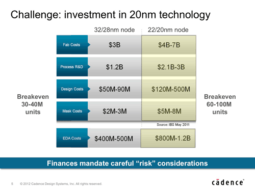
The A5 system on chip in the current Apple products, designed at 45nm, could come in under $1 billion to design and bring to market with effective control of the supply line. Cost projections for a chip at 28nm (the next step) could be as much as $3 billion. At 20nm, the cost could exceed $12 billion (if you build your own fab, which Apple could well afford.) The Cadence exec stated that the cost of EDA tools (both purchased and developed) could run as high as $1.2 billion alone.
The evidence of the increasing costs of development can be seen in the profit margins of the iPad. According to iSuppli, the cost of the A5 chip in the new iPads at $23 is double the cost of the original A4 chip. Why is the cost going so high? Because the way chips are being manufactured is changing dramatically.
Beckley explained that the physics of making a semiconductor mask reached a breaking point at the current most popular nodes as the resolution of a photoresist pattern begins to blur around 45nm. Double patterning was created to address that problem at 32nm. “But everyone wanted to avoid doing it at 32nm because of the mask costs. They wanted to maximize their investment in lithography equipment.”
The process splits the design where the structures are too close together, into two separate masks. It's an expensive process (especially when each mask costs around $5 million) and requires entirely new ways of creating the masks to avoid rule violations. But where the foundries were willing to let is slide at 35nm, they are requiring double patterning at everything below, Beckley stated.
These new techniques are driving up development costs straight up the design chain. Beckley said he has close to 400 engineers in his unit working on tools just for 20nm design — half of his entire staff.
The benefits of the moving the node are just as tremendous, he said. Instead of millions of transistors, each chip will have billions allowing for greater functionality in devices. “We expect improvements of 25-30 percent in power consumption and up to 18 percent overall perform and improvement,” he predicted.
“If what I'm saying scares you, it should. There are many questions and issues to be ironed out,” Beckley concluded. “But at Cadence we are already working with a dozen customers on active test chips, which will increase to 20 very soon, and we are already working with customers for products at 10
nm.”
■
Advertisement
Learn more about Footwasher Media


