
By Brian Santo, contributing writer
Holograms are so common in science fiction that it almost comes as a shock to discover that building a small, ultra-thin hologram display is impossible — or was until a few months ago. An Australian-Chinese research team recently busted through a fundamental barrier in materials science, creating hope that it might be possible to put holograms on digital devices such as smartphones.
The innovation was getting around a barrier in fundamental physics. The thickness of computer-generated holograms (CGH) has been generally limited to the optical wavelength scale in order to ensure adequate phase shift modulation, according to the paper published in May in the journal Nature Communications that describes the innovation. The spectrum of visible light is roughly 390 to 700 nanometers.
If electronics manufacturers are going to integrate holograms in their displays, however, they need them to be no more than a few nanometers thick.
That would have been an insurmountable gap, but it just so happens that there’s a class of materials with an unlikely set of characteristics that turn out to be strangely and inexplicably appropriate for solving the problem. (These days, it seems that there’s always a bizarro class of materials with an unlikely set of characteristics that turn out to be strangely and inexplicably appropriate for solving whatever problem anybody has. I mean, bulletproof Oobleck , anyone?)
Anyway, this particular class of materials is called topological insulators. These materials hold the low refractive index in the surface layer but the ultra-high refractive index in the bulk, which the researchers observe “makes them promising for designing novel optoelectronic devices, including nanometric holograms.”
The researchers are using an antimony-tellurium alloy (Sb2 Te3 ), and they’ve created a holographic thin-film (on a silicon substrate) that they say acts “as an intrinsic optical resonant cavity due to the unequal refractive indices in their metallic surfaces and bulk. The resonant cavity leads to enhancement of phase shifts and, thus, the holographic imaging.”
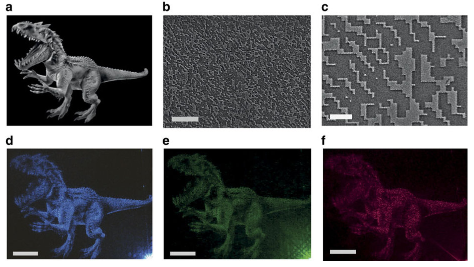
According to Nature : (a) The original image of the dinosaur. (b,c) Last printed hologram patterns. (d−f) Holographic renditions created by illuminating the nanometric holograms using 445-, 532-, and 632-nm continuous wavelaser beams.
The result is the ability to handle wavelengths from 350 to 1,000 nm — the full visible spectrum. The thin-film is only 60 nm deep, getting them a long way toward their thickness goal.
Making the material thinner — 25 nm — led to a lower-quality hologram, but other factors come into play, and the researchers say that they’re working on how to balance those factors to get a thinner thin-film with the least sacrifice in image quality.
They say that the manufacturing techniques are suitable for mass production.
The researchers posit a number of possible uses beyond holographic displays. These holograms might also be useful for data storage and security. For example, they can also be embedded in credit cards or even currencies as an anti-counterfeiting measure.
Advertisement
Learn more about Electronic Products Magazine


