Written By Brian Santo, contributing writer
Moore’s Law will fail in the next two device generations, or Moore’s Law will remain in effect for the foreseeable future. Which occurs depends on a lot of factors, the most important of which is how emotionally attached anyone is to silicon. Silicon is a dead end. But if other semiconductors qualify for the continuance of Moore’s Law? That would be a different story — then Moore’s Law keeps going. At least for a little while.
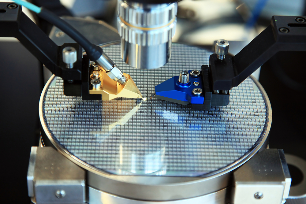
Researchers at Stanford University recently determined that hafnium diselenide (HfSe2 ) and zirconium diselenide (ZrSe2 ) have properties that make them possible successors to silicon.
Silicon has many properties that make it incredibly useful, but only a few are of note for our purposes here. One is that silicon has a “native” insulator that is easy to create: silicon dioxide (some wags note that silicon works so well because it rusts). Another property is a bandgap of 1.1 eV permitting low-voltage operation at reduced leakage current.
Semiconductor manufacturers are fabricating silicon chips at the 10-nm node. Silicon chips at the 7-nm node are due in later in 2018 or perhaps in the first half of 2019. Physicists believe that they might get to the 5-nm node with silicon.
Notionally, circuitry could be created at the atomic level, but the physics that electronic circuits rely on get fuddled by weird quantum effects before the circuitry gets reduced to atomic scale. Researchers are currently convinced that quantum wonkiness would kick in with silicon just past the 5-nm node, somewhere around 10 atoms thick.
The Semiconductor Industry Association’s official roadmap includes a short-term workaround. The industry expects that leading-edge manufacturing will abandon planar processing for 3D architectures, perhaps sometime around 2021. The technique is believed to have its limits, however.
Another option, then, is to go with some semiconductor other than silicon. The industry has been examining several as possible successors to silicon, including silicon germanium (SiGe), tungsten diselenide (WSe2 — which has intriguing optoelectronic properties ), molybdenum disulfide (MoS2 — a popular film lubricant), and black phosphorous. All have different shortcomings, often including the lack of a good insulator to pair with.
In fact, at smaller manufacturing regimes, silicon needs a better insulator to pair with. IC manufacturers have been increasingly replacing silicon dioxide with other thicker, more exotic insulators with higher dielectric constants (κ), the Stanford Researchers point out in their paper. SiO2 ’s is roughly 4, and the various high-κ replacements range from 16 to 20.
All of this is why alternatives to silicon are being explored. Researchers at Stanford University have determined that, similar to silicon, oxidation is possible with hafnium diselenide and zirconium diselenide, which is highly encouraging. HfSe2 and ZrSe2 also have bandgaps within range of silicon’s — 0.9 eV and 1.2 eV, respectively.
As the Stanford researchers assert in their paper , “These are the first 2D materials to demonstrate technologically relevant properties of silicon, in addition to unique compatibility with high-κ dielectrics, and scaling benefits from their atomically thin nature.”
Furthermore, both of these materials can be fabricated and retain ordinary device characteristics at a thickness of only three atoms deep, which is ultimately what will buy the IC industry a few more miniaturization steps.
It’s established that it’s not possible to get to atomic scale circuitry, but even were that not the case, IC manufacturers aren’t that far away from being at atomic scale anyway.
A single silicon atom has a Van der Waals radius of 210 picometers, or 0.21 nanometers, which translates into a diameter of about 0.42 nm — or roughly a twelfth of IC manufacturers’ target of 5 nm.
Selenium’s Van der Waals radius, meanwhile is 190 pm, or a diameter of about 0.380 nm. Stacking three of those gets you to 1.2 nm. (It appears that the values for zirconium and hafnium are as yet undetermined, but of the elements whose values have been determined, most are fairly close in size to silicon and selenium.)
That’s the improvement versus silicon, but the point remains that there isn’t all that much room left for scaling down circuitry based on any semiconducting element.
Advertisement
Learn more about Electronic Products Magazine


