Active area size, thermal resistance, output capacitance, and gate charge all figure into selecting the right device
BY ALEXANDER CRAIG
Fairchild Semiconductor, South Portland, ME
http://www.fairchildsemi.com
High-voltage MOSFET technology has undergone much change in the past few years, bringing the power supply engineer many options. Understanding the subtleties of the different MOSFETs and the stresses seen in different switching circuits helps engineers avoid problems and maximize efficiency. The implications of higher current density and faster switching speeds along with other aspects of MOSFETs beyond simple RDS(on) are important factors, as are some rules of thumb for replacing older MOSFETs with newer types.
Technologies
Two basic technologies are used with high-voltage MOSFETs: a more conventional planar technology like Fairchild’s QFET UniFET, and a new charge-balanced technology. Planar technology is very robust and durable, but has a much higher RDS(on) , for a given active area and breakdown voltage, than the charge balanced technology like Fairchild’s SuperFET or SupreMOS.
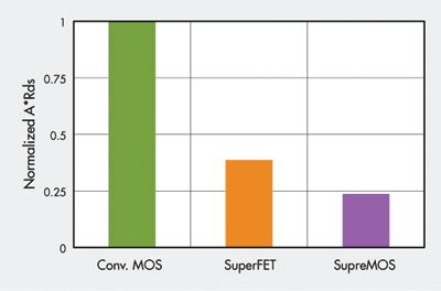
The dramatic difference in active area size for a given RDS(on) affects the devices thermal resistance and switching speed via output capacitance and gate charge. Figure 1 shows the on resistance of these three technologies.

Fig. 1. A comparison of three FET technologies.
The newest charge-balanced device had an RDS(on) that’s just 25% of the a conventional MOSFET with the same breakdown voltage and size. If one was only to look at RDS(on) one could wrongly conclude that they could use a MOSFET one-fourth the size of the conventional one. But, since the die size is smaller, its thermal resistance is higher.
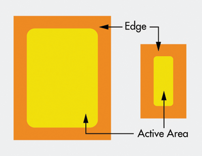
There are further implications of this when one considers that a MOSFET is more than just an active area represented by RDS(on) . It also has something called “edge terminations,” which prevents the device from having a voltage breakdown over the edge of the die. For smaller MOSFETs, this edge area can be more area than the active area in particular for high-voltage devices, as illustrated in Fig. 2 . While the edge area does not contribute to the RDS(on) , it does contribute to the thermal resistance (junction to case). So, at higher RDS , having a very small active area does not dramatically reduce the cost of the overall device.

Fig. 2. For a smaller MOSFET the edge area can be even larger than the active area.
A critical parameter
The junction temperature (Tj) is a critical parameter for any semiconductor device. Once you exceed Tj ( max) of a device, it will fail. Keeping Tj low will help make your system more efficient since higher junction temperature causes higher power losses because of higher RDS(on) , and worse reverse recovery time of the body diode. It is beneficial to understand what influences this and be able to calculate junction temperature. This is done with Eq. 1:
Tj = Ta + Pd * RøJA (1)
which consists of three factors: ambient temperature Ta , power dissipated Pd, and RøJA, the thermal resistance, junction to ambient. Pd consists of the conduction losses and the switching losses of the device. This can be calculated with Eq. 2:
Pd = D * RDS(on) * ID 2 + fsw * (Eon +Eoff ) (2)
The conduction losses represented by the first term are straightforward, where D is the duty cycle, ID is drain current, and RDS(on) is drain to source resistance, which is also a function of current and temperature. One should look at the data sheet for values at the approximate junction temperature and drain current conditions that the application is operating at for this value.
Getting the exact numbers for D, ID, and RDS(on) is often difficult, and engineers tend to pick the upper ends of a reasonable value. One might think that the only parameter that needs to be dealt with is RDS(on) , but in order to get a lower RDS(on) there typically needs to be a larger die, which influences switching losses and body diode recovery.
Switching losses
The second half of the power dissipation equation has to do with switching losses. It is written in a form that is more typically seen with reference to IGBTs, but the fsw * (Eon + Eoff ) are much more descriptive. Depending on the circuit, you may have no or very low turn-on losses.
These losses are influenced by the switching speed and recovering diode. In a planar MOSFET, it is much easier to improve the body diode performance through lifetime control than it is in a charge-balanced device. So, if your application requires the conduction of the body diode of the MOSFET, such as in a motor drive UPS or some ballast applications, improved body diode characteristics may be more benificial then the lowest RDS(on) .
These losses are multiplied by the switching frequency (fsw ). Properly designing the gate drive circuit is key, and the input capacitance is an important factor in that design.
Thermal resistance
Another key part of calculating the maximum junction temperature is the thermal resistance junction to ambient, RøJA , which is calculated from Eq. 3:
RøJA = RøJC + RøCS + RøSA (3)
RøJC is the thermal resistance junction to case and is related to die size. RøCS is the thermal resistance case-to-sink, which is related to the thermal interface and electrical isolation and is a user parameter. RøSA is the thermal resistance sink to ambient and is basically the heatsink and airflow.
Semiconductor datasheets typically provide one with a thermal resistance junction-to-case and, with isolated packages, the thermal resistance junction-to-sink. The thermal resistance junction-to-ambient is often provided, but this assumes there is no heat sink and that the device is mounted on the board in dead air or with a defined amount of copper for some surface-mount devices. In most cases, it is the responsibility of the power supply engineer to determine the thermal resistance case-to-sink and sink-to-ambient.
The importance of thermal resistance manifests itself in many ways including the current rating of a device, as can be seen in the table below. Three different 600-V devices, all of which are rated at 7 A, are shown, but each having three very different RDS(on) and RøJC values. Since the current rating of the MOSFET is purely a conduction loss equation, the impact of a lower thermal resistance is evident.

Fig. 3. Each available technology has advantages.
Therefore, selecting the correct device really depends on how you intend to use that device such as what switching frequency one intends to use, what topology and the thermal path of one’s application and, of course, what cost one wants to pay.
Some general guidance is that, in PFC and flyback applications that do not have body diode recovery losses, if RDS(on) is greater than 1 Ω, an advanced planar technology such as UniFET (II), QFET, or CFET tends to be a better solution. This is largely because the lower RøJC, helps keep the device cooler. For this higher RDS(on) requirement, the active area of the charge-bounced device takes a relatively small percentage of the total die area due to the edge termination and a planar MOSFET, even though a slightly larger piece of silicon, is a less-expensive process and the package cost is approximately the same.
For applications that do incur the reverse recovery, it is very important that diode characteristics be examined in addition to the RDS(on) and RøJC values. MOSFETs in both the advanced planar and charge-balanced technologies are offered with improved body diode characteristics.
In applications that require the lowest RDS(on) and fast switching, the new balanced devices such as SupreMOS and SuperFET offer the greatest advantage. Typically, a SuperFET offers the greatest advantage at RDS(on) requirements between 1 and 0.5 Ω, and the SupreMOS provides a significant benefit for below 0.5 Ω. This differentiation is again due to the thermal resistance contribution. ■
Advertisement
Learn more about Fairchild Semiconductor


