What could be more basic than a voltage reference—a simple, constant reference voltage? As with all design topics, there are tradeoffs. This article discusses the different types of voltage references, their key specifications, and the design tradeoffs, including accuracy, temperature-independence, current drive capability, power dissipation, stability, noise, and cost.
You can find voltage references inside almost any advanced electronic product, either standalone or integrated into larger functions. Understanding the technology as well as the system error budget is an important design consideration. Because of limited space, we suggest further reading in the footnotes as we touch on system concepts. For example:
1.In a voltage regulator, a reference provides a known value that is compared to the output to develop the feedback used to regulate the output voltage1.
a. Remote voltage adjustment and power-supply margining may be needed in the application2, 3, 4.
2.In a data converter, a reference provides an absolute voltage to compare to the input voltage to determine the proper digital code5.
a.Error budgets for an analog-to-digital converter (ADC) and a voltage reference; or digital-to-analog converter (DAC) and a voltage reference combination6.
b.Other data converter error sources, effective resolution, and number of bits7, 8.
c.Tools and calculators for converter accuracy and clock jitter, signal bandwidth, and THD9, 10.
3.In a voltage detector circuit, the reference is used as an absolute threshold to set the trip point11.
The required specifications depend on the application. This article discusses the different types of voltage references, their key specifications, and design tradeoffs. It offers information to help designers select the optimum voltage reference for their applications.
The Ideal
An ideal voltage reference has a perfect initial accuracy and maintains its voltage independent of changes in load current, temperature, and time. In the real world, a designer must make tradeoffs such as: initial voltage accuracy, voltage temperature drift and hysteresis, current source and sink capability, quiescent current (or power dissipation), long-term stability, noise, and cost.
Types of Reference
The two most common types of references are zener and bandgap12, 13. Zeners are usually used in two-terminal shunt topologies. Bandgap references are usually used in three-terminal series topologies.
Zener Diodes and Shunt Topologies
Zener diodes are diodes optimized for operation in the reverse-bias breakdown region. Because breakdown is relatively constant, it can be used to generate a stable reference by driving a known current in the reverse direction.
One big advantage of zeners is the wide range of voltages that are available, from 2V up to 200V. They also have a wide range of power handling capability, from several milliwatts to several watts.
The key disadvantages of zener diodes is that they are not precise enough for high-precision applications and their power consumption makes them a tough fit for low-power applications. An example is the BZX84C2V7LT1G, which has a breakdown, or nominal reference voltage, of 2.5V with a variation from 2.3V to 2.7V, or ±8% accuracy. This is suitable only for applications that need little precision.
An additional concern with a zener reference is the output impedance. Our example above has an internal impedance of 100Ω at 5mA and 600Ω at 1mA. A non-zero impedance causes an additional variation in the reference voltage depending on the variation in load current. Selecting a zener with low output impedance minimizes this effect.
Buried zener diodes are a specific type of zener that are more stable than a regular zener, due to their structure, which places them below the surface of the silicon.
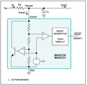
An alternative to an actual zener diode is an active circuit that emulates a zener. Circuitry allows the device to significantly improve upon the classic limitations of the zener. One such device is the MAX6330. It has a tight 1.5% (max) initial accuracy over a 100µA to 50mA variation in load. A typical implementation of this type of IC is shown in Figure 1.
 Figure 1. Using the MAX6330 as an active circuit that emulates a zener diode.
Selecting the Proper Shunt Resistor
All shunt configuration references need a current-limiting resistor in series with the reference element. It can be calculated from the following equation:
RS = (VIN(max) – VSHUNT (min))/(ISHUNT (max) + ILOAD(min)) ≤ RS ≤ (VIN (min) – VSHUNT (max))/(ISHUNT (min) + ILOAD (max))
where:
VIN is the input voltage range
VSHUNT is the regulated voltage
ILOAD is the output current range
ISHUNT is the minimum shunt operating current
Note that a shunt circuit always consumes ILOAD (max) + ISHUNT whether or not a load is present.
The same shunt can be used for 10VIN or 100VIN by properly sizing RS. Choosing the largest nominal resistor value for RS gives the lowest current consumption. Remember to provide a safety margin to incorporate the worst-case tolerance of the resistor used. You should also ensure that the resistor's power rating is adequate, using either of the following two general power equations:
PR = IIN(VIN(max) – VSHUNT)
= I²INRS
= (VIN(max) – VSHUNT)²/RS
Bandgap References and Series Mode Topologies
The key differences between a shunt and series reference is that the three terminal series-mode voltage references do not require an external resistor and have significantly lower quiescent power. The most common form is the ubiquitous bandgap reference.
Bandgap Basics
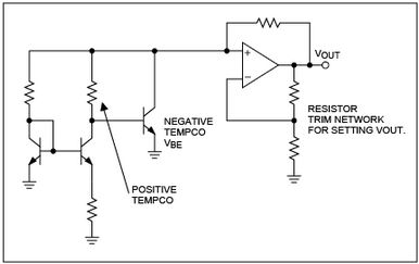
A bandgap reference develops two voltages: One has a positive temperature coefficient (tempco) and one has a negative tempco. Together, they have a zero-tempco sum at the output.
The positive tempco is usually derived from the difference of two VBE's running at different current levels. The negative tempco uses the naturally negative tempco of the VBE voltage (see Figure 2).
In practice, the tempco sum is not exactly zero. Depending on design details like the IC circuit design, packaging, and manufacturing test capabilities, these devices can usually achieve a VOUT tempco between 1 and 100ppm per degree C.
 Figure 2. Bandgap voltage reference.
Maxim’s Bandgap Reference Calculator (BGRC) Users Guide (in the Calculator zip file) allows one to simulate a Brokaw Bandgap reference cell. The effect of trimming the bandgap is shown for temperatures from absolute zero to 175°C. The curvature correction circuit is also adjustable to allow a design engineer to understand the reference IC design process. The physics behind the design becomes apparent along with an understanding of the resulting error waveforms and magnitude.
The use of either a shunt or series topology is typically dictated by the application and the desired performance. See Table 1 for some comparisons between zeners in shunt topologies and bandgaps in series topologies.
 Power Consumption
If you are designing a medium precision system like a high-efficiency, ±5% power supply or perhaps an 8-bit data acquisition system that requires minimal power, you could use a device like the MAX6025 or MAX6192. Both are 2.5V references that consume a maximum of 35µA. They have very low output impedance so the reference voltage is virtually independent of IOUT.
Source and Sink Current
Another specification is the reference's ability to source and sink current.
Most applications require a voltage reference to source current to the load(s) and, of course, the reference needs to be able to supply the required load current. It also needs to supply any IBIAS or leakage currents—their sum can sometimes exceed the load currents.
ADCs and DACs typically require between tens of micro-amps for a converter like the MAX1110, to 10mA (max) for devices like the AD7886. The MAX6101–MAX6105 family of references sources 5mA and sinks 2mA. For really heavy loads, the MAX6225/MAX6241/MAX6250 family sources and sinks 15mA.
Temperature Drift
Temperature drift is normally a correctable parameter14, 15. It is typically a very repeatable error. Correction can be accomplished by adding a calibration step or by reading a value from a look-up function that has been previously characterized.
Output Voltage Temperature Hysteresis
This parameter is defined as the change in output voltage at the reference temperature (+25°C) due to sequential but opposite temperature excursions (i.e. hot-to-cold and then cold-to-hot). Very negative effects can occur due to this effect since its amplitude is directly proportional to the temperature excursion the system underwent. In many systems this type of error is not very repeatable. This parameter is a function of design of the IC circuit as well as effects from the packaging. For example: The MAX6001 device in a 3-pin SOT23 has a typical temperature hysteresis of 130ppm. But a larger, more stable package, like the MAX6190 in the 8-pin SO, has only 75ppm.
Calibration16, 17, 18, 19, 20
Calibration is very common in high-resolution systems. In a 16-bit system, you need better than a 1ppm/°C reference for the commercial (0°C to +70°C) temperature range to stay within the ±1 LSB over the entire range, with a +25°C reference point. ΔV = (1ppm/°C × 5V × 45°C) = 255µV. This same temperature drift extended over the industrial temperature range is only acceptable for a 14-bit system.
Why one should calibrate, correcting component tolerance, gain, and offset16, 17.
Free calculators for ADC and DAC accuracy and thermal noise19, 20.
Design tools of simulation, decoupling capacitors, and filters (free or low cost)18.
Calibration circuit ideas, tips, and FAQs21, 22, 23, 24.
Noise
Noise usually consists of random thermal noise, but can also include flicker noise and other spurious sources. The MAX6150, MAX6250, and MAX6350 are all good choices for low noise applications with 35µV, 3µV, and 3µVP-P noise performance, respectively. All of these contribute less than 1 LSB of noise into your measurement. One could over-sample and average, but it comes at the cost of processor power and increased system complexity and cost.
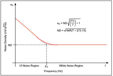
Maxim’s Thermal Noise Calculator (TNC) Users Guide (in the Calculator zip file) aids in the analysis of thermal noise found in resistors and other noise sources. TNC finds the noise voltage generated by any device if its white-noise spectral density and 1/f corner frequency are known. TNC can also be run on a HP 50g calculator or a PC using a free emulator program.
 Figure 3. Typical spectral noise density.
The thermal noise calculator can show the noise contribution for a customer over a specified bandwidth.
Long-Term Stability
This parameter is defined as a change in voltage over time. It is primarily due to die stress or perhaps ion migration that exists in a package or family of devices. It is important to note that the circuit board cleanliness can show up as a long-term change over time; especially over temperature and humidity. This effect, at times can be larger than the inherent device stability. Long-term stability is typically only specified at the reference temperature, usually +25°C.
Summary
The difficulties of designing any system lie in balancing the tradeoffs: cost, size, precision, power consumption, etc. It is important to consider all of the pertinent parameters when selecting the optimum reference for a design. It is interesting to note that many times a more expensive component can result in a lower total system cost due to the reduction in cost of compensation/calibration in manufacturing phase.
Advertisement
Learn more about Electronic Products Magazine


