Three of the most common design considerations prevent op-amp afterthought
BY GINA HANN
Texas Instruments, Dallas TX
http://www.ti.com
Operational amplifiers (op amps) play many different roles in optimizing the performance of mixed signal system design. Today’s mixed signal designer is challenged to understand the requirements of both the analog and digital portions of the signal chain.
With the diverse range of op-amp functions available, choosing the right one for each niche element in a mixed-signal design can be tricky. In fact, very often the need for an op amp is not recognized until after board layout or even the first prototype, resulting in an expensive and time-consuming redesign. You can avoid this costly situation of “op-amp afterthought” with a little bit of planning.
Looking at a classic analog signal chain consisting of a input signal-conditioning amplifier to digital converter to processor, there are some well-known functions for op amps front-end signal conditioning and analog output signal conditioning. But there are a number of other opportunities where amplifiers can play a key role for improving the accuracy and performance of your mixed-signal design; and a number of opportunities for op-amp afterthought to occur.
Rule 1. Know your sensor input before you choose an op amp or instrumentation amp, and know the output requirements of your conditioning amplifier.
One of the most disappointing cases of op-amp afterthought occurs upon realizing that the wrong input amplifier was selected for the job, or that after carefully selecting the appropriate amplifier for the sensor, an additional amplifier is needed to maintain system precision and accuracy.
Design considerations
So what are the design considerations when choosing an amplifier for sensor signal conditioning? The sensor impedance, sensor output voltage span, common mode signal levels and type of excitation required all influence proper amplifier selection.
If a very-high-impedance sensor is being used, such as a pH sensor, then it is critical to choose an amplifier with extremely low input bias currents so that dc errors across large impedance changes are minimized. If the output voltage span is a few millivolts as with many bridge sensors, a low offset and most likely low-drift op amp or instrumentation amplifier will help to avoid losing the input signal in the midst of proportionally larger input errors of the amplifier.
Once you select an appropriate signal-conditioning amplifier, take time to consider the demands on the output of that amplifier. If you are planning for digital signal acquisition, what is the equivalent input capacitance and sampling frequency of the converter? If the signal-conditioning amplifier lacks sufficient bandwidth to settle to a desired accuracy within the sampling time of the converter, an additional higher-bandwidth drive amplifier may be needed.
Many board- and system-level designers realize this unfortunate truth in the latter stages of development. Thus, the need for a drive amplifier at the signal output conditioning stage becomes the first culprit for op amp afterthought.
Rule 2. When optimizing an instrumentation or difference amplifier for accuracy, pay careful attention to the reference pin.
Not every design is driven for the highest possible system accuracy, but it is always a good idea to have an understanding of the minimal amount of accuracy your design can tolerate. If you are designing with an instrumentation or difference amplifier, you have probably selected your device because of a combination of gain accuracy, high CMRR, low drift, and low noise. While these are important specifications for overall system accuracy, don’t let your hard work go to waste – op-amp afterthought will happen if you neglect to account for how the reference pin influences the amplifier output voltage.
Difference amplifiers are at the heart of many instrumentation amplifier topologies, so for simplicity we will look at the influence of the reference pin on a difference amplifier. The output voltage of a unity gain difference amplifier is as follows:
VOUT = (VIN+ – VIN¬ ) + VREF
For single-supply systems, the instrumentation amplifier REF pin is optimally biased to mid-supply to achieve maximum symmetric output swing. The above equation shows that errors on VREF will translate to direct error at the output. It is important to ensure that an accurate voltage is applied to the REF pin.
When creating a reference voltage for the difference amp, for reasons of cost and simplicity, many designers use an available supply from which they achieve a desired reference voltage with a cheap resistor divider. While this may seem like an efficient use of available supplies and be an easy enough solution, a case of op amp afterthought is waiting.
The difference amplifier REF pin requires a low-impedance source to avoid a divider error with the internal difference scaling resistors. By using a divider that applies a relatively high impedance to the reference pin, an error is introduced at the output of the difference amplifier.

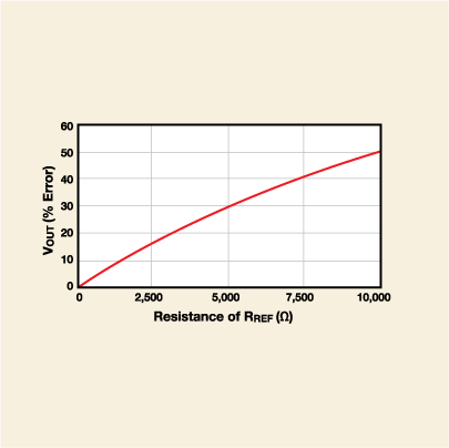
Fig. 1. Basic difference amplifier with series resistance at the REF pin (modeled by RREF ) creates a voltage divider error (a). Percent output error due to increasing series resistance at REF pin for fixed values of VIN+ and VIN– (b).
Figure 1a shows the basic difference amplifier topology with R = 10 kΩ and a modeled equivalent resistance (RREF ) used to represent the impedance introduced by a voltage divider. With the introduction of additional impedance at the REF pin, the output voltage equation now becomes:
VOUT = [2VIN+ ( R+RREF )/(2R+RREF )] – VIN -]
Based on the original output voltage equation, it is apparent that the role of RREF can be significant. Figure 1b describes the total error as a percent of ideal output voltage resulting for resistances from 1 Ω to 10 kΩ. Depending on the equivalent impedance seen at the REF pin, an error of up to 50% of the actual voltage output value can result.
This situation can be avoided by introducing a buffer (as shown in Fig. 2 ) to drive the REF pin to a known and stable value. The low closed-loop output impedance of a buffer will maintain the overall accuracy of the difference amplifier.
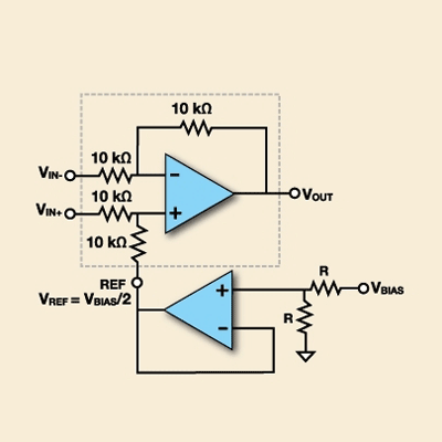
Fig. 2. Basic difference amplifier with buffered REF pin.
Rule 3. Understand the role of the ADC voltage reference for accurate digital conversions.
The issue described in Rule 1 is circumvented by an amplifier with sufficient bandwidth to keep up with the charge demands of the input switching on certain data converters. The same is true with Rule 3 – one must also consider the effect of input switching and sampling with respect to the voltage reference used by the data converter.
For data converters with integrated references, this may not be an issue. But if you are using an external voltage reference to accurately bias your data converter, you can avoid op-amp afterthought by evaluating the need for a reference buffer early in your design process.
The internal switching frequency common to successive-approximation register (SAR) converters requires a constant charge to maintain the accuracy of the data converter. By choosing an amplifier with sufficient bandwidth and noise to drive the reference to an accurate final voltage within the acquisition time of the data converter, you can pat yourself on the back for once again not becoming a victim of op-amp afterthought. ■
Advertisement
Learn more about Texas Instruments


