By way of random discovery, Jim Edgar, a Kansas State University distinguished professor of chemical engineering, has created a whole new way of building better semiconductors.
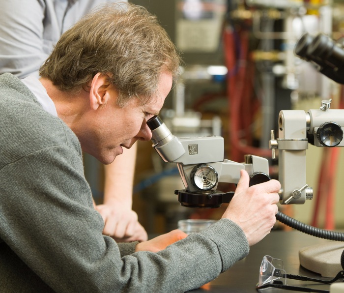
Edgar’s new process stands to significantly benefit the power electronics industry as well as manufacturers of semiconductor devices. He explained his approach using cake as an example.
“It's like a stacked cake separated by layers of icing,” Edgar said. “When the layers of semiconductors don't match up very well, it introduces defects. Any time there is a defect, it degrades the efficiency of the device.”
In short, Edgar’s approach improves upon how semiconductors are layered; it’s done in such a way so as to minimize potential defects. The potential of this process was first realized in 2011 when Yi Zhang, a doctoral graduate in chemical engineering, was working in the University’s laboratory and found a substrate sample that was very smooth.
Upon review of the material, collaborative researchers at the State University of Stony Brook and the University of Bristol (United Kingdom) confirmed the layer’s presence and proved that it few defects than on the standard substrate.
“We have applied this process to other systems,” Edgar said. “We are working on verifying that it is not just these specific materials we started with, but that it can be applied to a lot of different materials.”
In the meantime, Edgar has received a patent for the process, which is referred to as “Off-axis silicon carbide substrates”. The abstract from the patent reads as follows:
A method of epitaxial growth of a material on a crystalline substrate includes selecting a substrate having a crystal plane that includes a plurality of terraces with step risers that join adjacent terraces. Each terrace of the plurality or terraces presents a lattice constant that substantially matches a lattice constant of the material, and each step riser presents a step height and offset that is consistent with portions of the material nucleating on adjacent terraces being in substantial crystalline match at the step riser. The method also includes preparing a substrate by exposing the crystal plane; and epitaxially growing the material on the substrate such that the portions of the material nucleating on adjacent terraces merge into a single crystal lattice without defects at the step risers.
Edgar’s latest work focuses on two different boron compounds: boron phosphide and icosahedral phosphide.
Via K-State
Advertisement
Learn more about Electronic Products Magazine


