Series or parallel LEDs in white-LED backlighting
BY TRAVIS EICHHORN
National Semiconductor
Santa Clara, CA
http://www.national.com
White LEDs used in backlighting provide illumination for the pixels in liquid crystal displays. The LEDs are typically routed on one or two sides of the displays light diffuser, and biased with 20 mA (VF = 3.6 V typ). Power gets to the LEDs in many ways. In a display using eight-LEDs you can have a string of 8, two strings of 4, four strings of 2, etc. For a given number of LEDs there can be more LEDs in parallel (lower voltage) or more LEDs in series (higher voltage). Both configurations have their advantages and disadvantages and sometimes combining both is the optimized design.
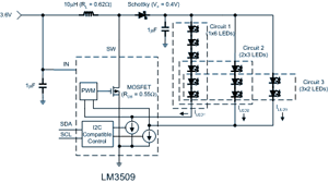
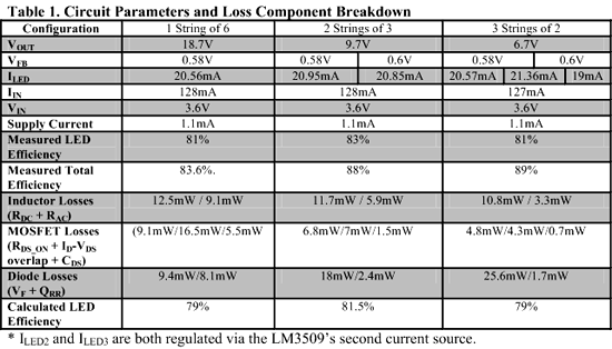
Take for example three different circuits: a single string of six LEDs, two-strings of three LEDs, and three strings of two LEDs, biased with 20 mA/LED from a 3.6-V source. The LED supply is a dual output, single inductor supply (LM3509) switching at 1.25 MHz (see Fig. 1 ). The LEDs are from Nichia (part #NSSW008C, VF is 3 V at 20 mA). Table 1 shows a breakdown of the three configurations.

Fig. 1. Many variations exist how power gets to LEDs.

Table 1. Circuit Parameters and Loss Component Breakdown
The main advantage to the 1 x 6 LED configuration is the single line for LED bias. Not so obvious is the better efficiency in the lower voltage configurations. A rough calculation using DC losses for the inductor (Iin 2 x RL ), the MOSFET (IIN 2 x RDS(on) x D), the diode (VF x ILED ), the current source (VH- x I LED ), and the supply current (ISW x VIN ) estimates the efficiency at 91% for the 1 x 6 configuration, 87% for the 2 x 3 configuration, and 83% for the 3 x 2 configuration.
This leads to an erroneous conclusion that the higher voltage circuit is more efficient due mainly to the VH_ /VOUT ratio. The analysis ignores two factors; the rms currents and the switching losses in the diode, MOSFET, and inductor.
To correct the previous calculation using rms currents the MOSFET loss becomes:
RDS x (ISW-RMS + IIN x √D(1 + IRIPPLE2 /(12 x IIN 2 )))2
and inductor loss becomes:
RL X (IL_RMS = IIN x √(1 + IRIPPLE 2 /12 x IIN 2 )))2
MOSFET switching losses
The MOSFET switching losses occur during the MOSFET turn-on and turn-off. The first component, ID-VDS overlap, causes periods of high power dissipation as the inductor current and output voltage simultaneously appear across the MOSFET between on and off states. The second component is power loss from charging the drain to source capacitance (CDS ) each switching cycle.
To understand ID-VDS overlap loss, consider the MOSFET in the LM3509. At the end of the off-time (VDS = VOUT + VDIODE ). The MOSFET driver begins charging the gate to the threshold voltage (VGS_TH ). When VGS_TH is reached the MOSFET current begins increasing while VDS remains at VOUT + VDIODE . From VGS_TH up to a point called the Miller plateau the current continues to increase.At the Miller plateau voltage VGS stalls due to the charging of the Miller capacitance (CGD ) which has its gate side trying to charge to the driver voltage and its drain side to GND. During this time VDS ramps down while the MOSFET conducts the inductor current. From the point of view of the drain (SW on the LM3509) the voltage approximates a rectangular waveform with a finite slew rate. This slew rate on both turn-on and turn-off results in brief periods of high power dissipation across the switch. This is approximated as
VOUT x IIN x (tRISE + tFALL )/2 x fSW
Figure 2a shows the rise and fall transitions for the 6 series example and the dual 3 series configuration. The higher voltage and longer transition times in the 6 series case result in more power dissipation.
facnnat2jun2007Fig. 2. MOSFET and diode switching losses.
The CDS loss is simply the energy into CDS every switching cycle
(CDS x VOUT2 x fSW )/2
Diode switching losses
Diode switching losses are mainly from charging the diodes capacitance during its blocking phase. This power loss is approximated as
QRR x fSW x VOUT
QRR is reverse recovery charge and is commonly given in the diode datasheet or in a curve of total capacitance vs. reverse voltage (QRR is the area under the curve). Figure 2b shows the typical diode reverse recovery charge in the 1 x 6 configuration and the 3 x 2 configuration.
The switching loss (or ac loss) in the inductor is mainly from core loss and skin effect. This information is often not available although the LPS3008-103 from Coilcraft does give this parameter and provides insight for switching losses in typical power inductors. The ac loss information is given in a graph of equivalent series resistance vs. frequency and is a resistive representation of the core loss and skin effect.
Core power loss
Core power loss, the difference between energy stored in the inductor’s core during the on-time and what is released during the off-time makes up the bulk of the switching loss. Core loss is dependent on inductor geometry, core material, and peak to peak current ripple. The major core loss component (hysteresis loss) increases with increasing peak to peak magnetic flux density (∆B). Every switching cycle the core magnetic flux density transitions a ∆B exhibiting some hysteresis which generates the familiar hysteresis loop for magnetic materials. The area of this loop multiplied by the switching frequency is the power loss. Core loss increases nonlinearly with ∆B and is a direct function of inductor voltage, shown by Faraday’s law in terms of magnetic flux density:
VL (t) = n x Ac x dB(t)/dt
where n is inductor turns and Ac is core area.
Using the approximation VL (t) = L x ∆IL /∆t, the previous equation is rewritten giving the approximation
∆B = ∆IL x L/n x Ac
Showing how ∆B and subsequently core power loss increases with higher current ripple.
The skin effect results from ac currents inducing a magnetic flux in the conductor which in turn induces opposing currents that counteract the original current. The opposing currents are higher at the conductor’s center, which essentially pushes the ac current to the surface of the conductor causing a higher ac resistance. The higher resistance is only a loss due to the ac currents.
Both the core power loss and skin effect increase with increasing inductor current ripple resulting in higher switching losses at larger VOUTs . From the LPS3008 datasheet, the 10-µH inductor shows around 2.3 Ω of ESR at 1.25 MHz. The inductors switching loss is the rms current ripple multiplied by this ESR:
RESR x (IRIPPLE /2√3)2
Table 1 shows a breakdown of the loss components for the three circuits giving a better estimate of the efficiency. Comparing the 1 x 6 LEDs to the 2 x 3 LEDs the switching losses in the higher-voltage circuit drastically reduce the efficiency from what was calculated using just dc analysis. Higher output differentials such as 12 series LEDs compared to three strings of four would see a more sizable difference. Additionally, the increased output capacitor size at the higher voltage makes the circuits larger and costlier.
The three examples make a strong case for choosing some combination of series and parallel LEDs over a single string. Factors such as component values, capacitances, and resistances might make a sweet spot for an output voltage that optimizes efficiency and component costs. Finally, as a boost converter’s output voltage increases the off time must decreases. Consider 1 x 10 LEDs compared to 2 x 5 LEDs. Using traditional 3.6-V LEDs at 20 mA VOUT will be 36.5 V and 18.5 V respectively. Assuming 80% converter efficiency for both and fSW = 1.25 MHz, the off time for the higher voltage circuit is approximately 64 ns and the lower-voltage circuit is approximately 125 ns. (tOFF = (1-D)/fSW and (1-D)=VIN /VOUT x efficiency.
At VIN = 2.5 V the off times move to 44 and 87 ns. Depending on the turn-on and turn-off times of the switch and the reverse recovery time of the diode, it might become impossible to regulate 10 LEDs, whereas longer off times in the dual 5-LED configuration allow for a larger margin of error.
Advertisement
Learn more about National Semiconductor


