Signal paths in 3G and feature/smart phone apps
Circuit requirements are unique in portable charger and data cable applications
BY JEFF JU and GERALD JOHNSTON
Fairchild Semiconductor
South Portland, ME
http://www.fairchildsemi.com
Application-specific signal path products are finding more and more relevance in 3G and feature/smart phone applications where higher-throughput video and USB data dominate. Several unique solutions illustrate this need and this article will offer suggestions that can shorten design time.
USB charger OVP compliance and plug-in detection
With the market moving to a single USB connector for both charger and data connections, there is strong potential for application-specific USB devices that not only focus on charger detection, but also offer excellent signal integrity. The new Chinese USB charger standard requires over-voltage protection of 6 V for the VBUS charger input. It calls for a device to be able to detect both this VBUS input OVP threshold and undervoltage conditions.
In such applications, the charger-detect function can find a short-circuit condition between D+ and D- lines for standard chargers and limit the charge current. There are many ways to implement the charger detection function, including the discrete solutions which use of the baseband processor’s A/D converter. But all those solutions have limitations in parasitic capacitance (>3-pF input gate capacitance typically) if those discrete detection ICs are wired directly onto the D+/D- lines.
Figure 1 is a thoughtful solution for this design challenge. It can detect the short between D+/D bus lines, and can tolerate all potential skews in the data mode particularly for long cable applications. Its low-load capacitance (
Also desirable in such applications is the integration of the power switch for turning on/off the charger path and the over/under voltage protection of VBUS input. For this application, the IC should be placed as close as possible to the USB controller output to reduce the signal reflection for an optimal data eye opening. Sometimes, designers can adjust the bias resistor of the controller output for improved signal integrity.
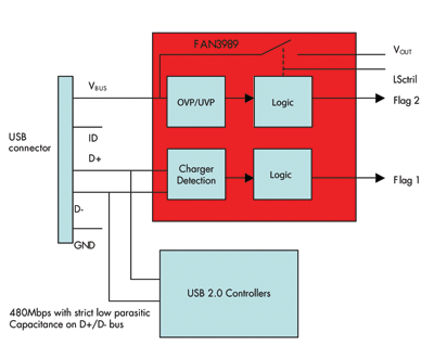
Fig. 1. A USB over-/undervoltage protection IC with charger detection can simplify a USB 2.0 high-speed interface.
USB connector sharing for TV phones
Single USB connector phones are becoming dominant in the market for universal adoption in both charger and data cable applications. This is further validated by the marketing trend in the ramp of TV phones for mobile video broadcasting. The TV output format typically uses the composite video format (CVBS).
Many portable encoders have limited maximum current output capability due to the total 150-Ω video load including a far-end 75-Ω termination resistor at the TV input. Additional video filter/driver functions are needed, but the output pins are limited (5-pin for USB connectors). This situation poses a challenge for designers on how to effectively multiplex those output signals without sacrificing the signal integrity under different working modes.
These modes include voice communication with microphone input, MP3 output with audio L/R channel, USB data of active D+/D- line communications requiring ultra-low parasitic capacitance on the lines, and the video mode with or without audio. All of these design challenges are solved using a single IC (see Fig. 2 ) that can route the microphone path, audio output path, video input/output path, and USB data bus with no interference between them. The audio path (L and R) must be able to handle the negative signals of up to 39 mW for headphones. The ac-coupled video output is recommended for low DC power consumption in portable applications.
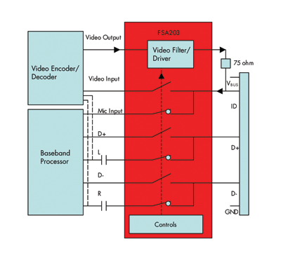
Fig. 2. USB connector sharing circuit is used in TV phone designs.
Dual-camera applications for 3G phones
As 3G technology becomes more mature, it will feature strong video conference capability with faster throughput. This capability will necessitate a higher-resolution camera for personal picture taking with a lower-resolution camera for video conferencing.
For flip or swivel phone designs, both camera modules are probably located at flip side due to limited space in base side with base-band and application processors. This presents challenges for designers since double wires can be required if not accommodated properly. This is even a more daunting design challenge for camera modules without high-impedance states under non-active and power down mode.
Figure 3 shows a nice solution for such applications using parallel-to-serial technology. Two serializers sit at flip side of the phone with a single serializer at base side.
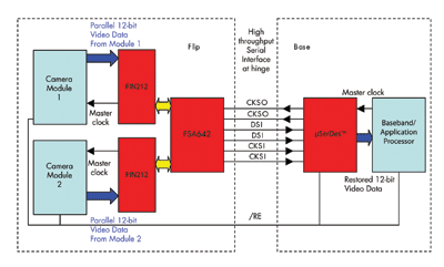
Fig. 3. Unique µSerDes and wide bandwidth switches aid dual camera applications.
The total number of wires that pass through the hinge is reduced to at most three-pairs (differential). The serializer converts all parallel YUV data into fast serial interface signals and the deserializer converts them right back to parallel format for the application processor camera I/Os.
A dedicated high-performance switch sits on the serial lines to change between picture and video conference mode. The wide bandwidth characteristics and ultra-low skews between the channels of this kind of switch facilitate optimal switching. This device handles the high-throughput differential signal without set-up/hold time problems, due to its fast propagation delays.
In such applications, special attention needs to be paid to the matching the length of serial lines in the layout. Minimal vias on differential lines are recommended to avoid the impedance changes. Impedance match is important for differential signals for high signal integrity particularly under high-data-throughput conditions for high-resolution camera with fast pixel clock and data rates. ■
For more on signal paths, visit http://www2.electronicproducts.com/AnalogMixICs.aspx.
Advertisement
Learn more about Fairchild Semiconductor


