Achieving high performance with clean supply rails is one of the greatest engineering design challenges
BY BRIAN HUFFMAN
Sr. Strategic Application Engineer,
ROEL VAN ETTINGER
Sr. Staff IC Design Engineer, and
CHRIS GATER, IC Design Director,
Micrel
www.micrel.com
With the vast uptake in portable connectivity devices and the ever shorter design cycles, competition is fierce. The noise performance of the power supply is vital and needs to be of extreme importance for designers of these new sensitive products. One of the greatest challenges for engineers in achieving high performance in their designs is that of the cleanliness of the supply rails.
Traditional power design processes for global positioning systems (GPS), cellular phones and image sensors are simply not good enough for the performance levels required today. In GPS applications, the receiver is highly sensitive and may need to decode very low power signals in the order of 160-dBW. Power supply noise increases the GPS signal acquisition time and reduces position accuracy. In a cellular phone, supply noise causes dropped calls due to a reduced signal to noise ratio.
Camera modules and image sensors require very wide dynamic range, operating at daylight condition to dark at night. Image sensors benefit from a clean power supply with greatly improved signal-to-noise ratio delivering higher image quality. In noise-sensitive systems, additional power supply filtering is a vital engineering consideration to address stringent design requirements.
Power supply filtering has traditionally been achieved by utilizing a simple LC filter in the supply line. The purpose of the filter is to reduce the switching regulator’s ripple voltage. With skilled board (PCB) layout, the output ripple of a buck regulator is typically 1% of the output voltage. A 2.5-V output can achieve 25-mV output ripple. The LC filter is designed to attenuate the switching regulator output ripple. A simple output filter can reduce this noise anywhere from a factor of ten (20 dB) to one hundred (40 dB); any high-frequency “spikes” that may be superimposed on the ripple are attenuated even more.
To achieve sufficient suppression with a single pole LC filter, a low cut-off frequency design is required resulting in a large value inductor and capacitor which is a bulky solution and not appropriate for modern low-footprint, low-profile designs. In portable applications a semiconductor switch is also required to save power, further increasing PCB board area.
For these highly sensitive and space-constrained end products, a more comprehensive and greatly reduced footprint solution is necessary to be able to develop a product matching or exceeding the expectation of the modern market.
Single-chip solution
Ripple Blocker technology (patent pending) enables a single-chip solution that combines an active filter and switch into one part. The PCB footprint is reduced over 65%, providing excellent performance (see Fig. 1 ) . The technology can also be applied to a low-dropout linear regulator (LDO) to achieve unmatched power supply rejection ratio (PSRR) performance from dc to 10 MHz.
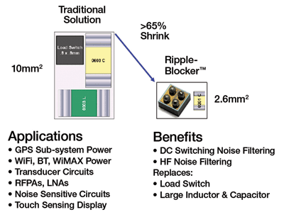
Fig. 1: MIC94300 board-space reduction.
The MIC94300 simplifies the filter design integrating a load switch in conjunction with an active filter circuit to provide an extremely clean output voltage. The load switch is controlled by an active-high enable pin. Forcing the enable low turns off the load switch and sends it into a near ‘zero’ off-mode current state. When enabled, the load switch is biased near its saturation region to maintain optimum performance between low Rdson and ripple rejection. The result is approximately a 170-mV fixed voltage drop between the input and output voltage. The MIC94300 is fully protected from damage due to fault conditions, offering linear current limiting and thermal shutdown.
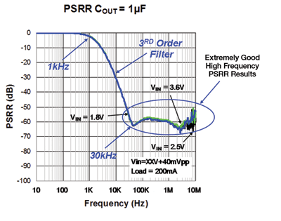
Fig. 2: MIC94300 ripple blocker performance
The MIC94300 attenuation factor is about 1,000 (60 dB) from 30 kHz to 10 MHz, a 10-fold improvement. The internal active filter passes dc and blocks any ac components with a frequency beyond 1 kHz. A third-order filter provides a steep rolloff; most of the attenuation is available from 30 kHz to 10 MHz. Virtually all switching regulator output ripple components will be reduced by about 60 dB, which is an improvement in design margin in any portable design.
A low 170-mV drop is maintained over varying loads, optimizing power efficiency. Most available LDOs will not produce this level of power supply rejection (PSRR) for such a small voltage drop over such wide bandwidth while consuming just 138 µA of ground current.
The magnitude of the output voltage ripple depends upon the inductor ripple current, the output capacitance value and its effective series resistance (ESR). A 25-mVp-p ripple has been achieved across the output capacitor. The fundamental frequency of 314 kHz is the switching frequency of the buck regulator, with harmonics being multiples of the switching frequency.
Figure 3 shows a MIC94300 block diagram . It combines the low RDS(on) of a current limit switch with the PSRR capability of an LDO. First, the LDO maintains a fixed voltage drop of 170 mV that is independent of load current. The voltage drop is set by an internal 170-mV voltage referenced to the input voltage. A low-pass filter passes the dc and blocks the ac component of the input voltage. The filtered signal is provided as a reference to the LDO so the output will follow the dc of the input but rejects any ac signal. The use of an NMOS as a pass device provides an extremely low dropout as used in current-limited switches.
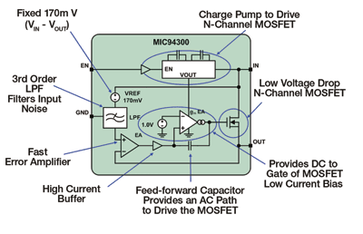
Fig. 3: MIC 94300 ripple blocker detailed block diagram.
The technology can also be applied to low-dropout linear regulators (LDOs) to produce a fixed output voltage with high PSRR from dc to 10 MHz. The output voltage is regulated like a traditional LDO regulator where the output voltage is set by a resistor divider network connected between the output and ground.
Standard p-channel LDOs have high PSRR at dc, but will start losing ripple rejection above 10 kHz. This rolloff is caused by the gain-bandwidth limit of the error amplifier.
The MIC94310 does not have this limitation because it uses an NMOS pass device.
Therefore, at higher frequencies where the loop gain drops, an NMOS pass device can still maintain a good PSRR. The MIC94310 surpasses the performance of a standard LDO at frequencies from 1 kHz to 10 MHz. This makes the MIC94310 a perfect choice to use as a regulator with a switching regulator input voltage whose switching frequency is typically in the 500-kHz to 3-MHz range.
The use of a high-Q LC filter to clean up the supply can cause unwanted and prolonged ringing when applying a load step, potentially leading to all kinds of interactions that are hard to debug during development. This is not the case when using any of the Ripple Blocker technology devices thus potentially reducing time to market.
Ripple Blocker technology provides a simple, space-saving, and low cost solution for dramatically reducing power supply noise. It offers substantial noise reduction due to a typically 60-dB PSRR performance up to 10 MHz in combination with only 170-mV voltage drop for the MIC94300 and 40-mV voltage drop for the MIC94310 at 200-mA load. ■
Advertisement
Learn more about Micrel


