Silicon carbide MOSFETs: Superior switching technology for power electronics applications
SiC offers many superior properties to Si for the construction of power switching devices
BY BOB CALLANAN
SiC Power Products Applications Engineer
Cree, Durham, NC
www.cree.com
In power electronics applications, the compound semiconductor silicon carbide (SiC) has been demonstrated in published literature [1 ] to be a superior material to silicon (Si) in many properties for the construction of power switching devices. Silicon carbide exhibits a critical breakdown field approximately 10X that of silicon; enabling the development of a thinner device structure for a stated breakdown voltage, which in turn reduces the on-resistance per unit area of the device by some two orders of magnitude compared to a silicon device. This higher breakdown field also enables the development of SiC MOSFETs with voltage ratings as high as 10 kV. [2] Silicon carbide also has a thermal conductivity 2.8X higher than silicon, providing a much higher current density at a given junction temperature than a comparably-rated silicon device. With a bandgap that is approximately 3X wider than silicon, SiC devices also exhibit significantly lower leakage current at high temperature operation – by more than two orders of magnitude.
By comparing both an existing 1,200-V Si switching device with a 1,200-V SiC MOSFET, the advantages of silicon carbide can be clearly demonstrated. In Figs. 1 and 2 , the forward conduction characteristics of Si MOSFETs, trench field stop (TFS) IGBTs (Insulated Gate Bipolar Transistors), non-punch-through (NPT) IGBTs are compared with those of SiC MOSFETs at 25C and at 150C.
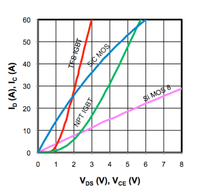
Fig. 1: Forward conduction characteristics at Tj = 25C.
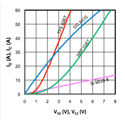
Fig. 2: Forward conduction characteristics at Tj = 150C.
As shown in Fig. 3 , the silicon MOSFET’s normalized on-state resistance (RDS(on) ) increases by more than 250% from 25C to 150C, while the RDS(on) of the SiC MOSFET increase just 20% over the same temperature range. The impact of this characteristic on the thermal design of a power electronics system is significant, including the reduction of up to 50% of the thermal management hardware (fans and/or heatsinks).
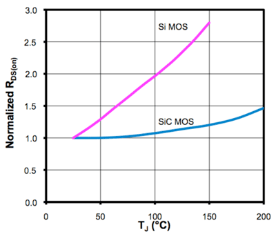
Fig. 3: Normalized RDS(on) vs temperature
The SiC MOSFET, as a majority carrier switch, effectively eliminates the minority carrier current tail experienced with silicon IGBTs, resulting in much lower switching losses and facilitates much easier paralleling of switching devices. Inductive switching characteristics (turn-on & turn-off losses) over the operating temperature range of the two types of devices is demonstrated in Fig. 4 , with the SiC MOSFET exhibiting significantly lower switching losses than silicon devices.
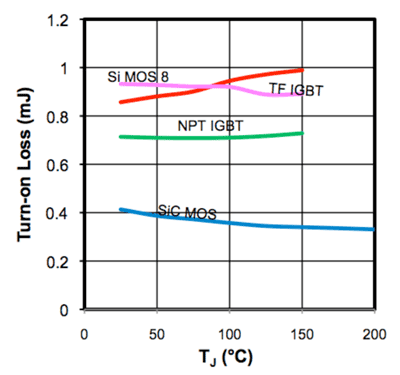
Fig. 4a: Turn-on switching loss vs. temperature comparison (VDD = VCC = 800 V, ID = IC = 20 A, RG = 10 Ω)
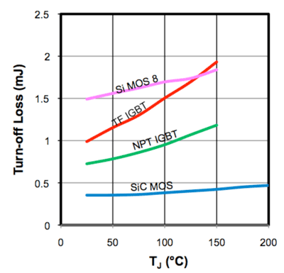
Fig. 4b: Turn-off switching loss vs. temperature comparison (VDD = VCC = 800 V, ID = IC = 20 A, RG = 10 Ω)
At the 1,200-V rating, SiC MOSFETs may be specified in virtually any application that currently employs 1,200-V silicon IGBTs, especially for those applications requiring higher operating frequency and higher system efficiencies. Figure 5 graphically depicts the application area for SiC MOSFETs vs. silicon IGBTs, including solar power inverters, wind turbine inverters, motor drives, induction heating systems, as well as high voltage dc/dc converters.
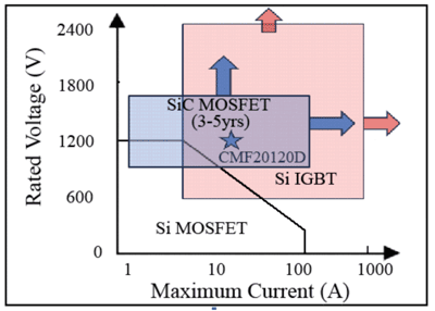
Figure 5: SiC MOSFET Application Areas
There are two design characteristics that must be observed when applying SiC MOSFETs in a power electronics circuit the elimination of the turn-off tail current exhibited by silicon IGBTs; and a modest transconductance that needs to be factored into the gate drive circuit design.
Although the elimination of the tail current is a significant advantage of the SiC MOSFET over the silicon IGBT, it is also critical to take into account that the IGBT’s tail current does have the effect of dampening parasitics during turn-off. This can lead to overshoot and increased ringing in the circuit when the IGBT is replaced directly with a SiC MOSFET. In some cases, additional voltage overshoot may be high enough to cause damage to the device; therefore it is vital to design sufficient snubber circuits to manage output interconnection parasitics and prevent the ringing from reaching damaging levels.
Compensating for the modest transconductance in the SiC MOSFET requires that gate-source voltage (VGS ) must be 20 V to ensure optimal performance from the device. This transconductance characteristic can also impact the transition between where the MOSFET operates as a voltage-controlled resistance device to where it becomes a voltage-controlled current source, as a function of VDS . This transition will typically occur at higher VDS values than with conventional silicon MOSFETs or IGBTs, which can in turn impact any anti-desaturation circuitry if the design takes into account the lower forward voltages where the device enters the constant current region.
The transconductance effect must also be considered in the gate drive circuit design, most notably in the requirement that the gate driver be capable of voltage swing of 22 V or higher (for example, a recommended on-state VGS of +20 V, with an off-state VGS of −2 or −5 V). Note that although the total gate charge of the SiC MOSFET device is significantly lower than in conventional silicon devices, this gate voltage swing is higher than in most silicon MOSFETs or IGBTs; however, the product of the gate voltage swing and the gate charge is still lower for the SiC MOSFET when compared to silicon devices of similar ratings. To achieve fast switching times, the gate voltage requires extremely fast dV/dt, thus a low-impedance driver is needed.
Careful consideration must be given to controlling the fidelity of the gate drive pulse, requiring a nominal threshold voltage of 2.3 V when the device is not fully on (dVDS/dt ≈ 0), until gate-source voltage reaches 16 V or higher. Because this range is considerably wider than with conventional silicon switching devices, the net result is that the SiC MOSFETs exhibit a slightly lower noise margin. Gate resistance should be carefully controlled to adequately dampen the gate drive pulse, thus eliminating excessive ringing on the gate drive signal that could lead to partial turn-off or unintentional turn-on of the MOSFET. The first order gate circuit is approximated in Fig. 6 , depicting a voltage pulse driving a simple series RLC circuit.
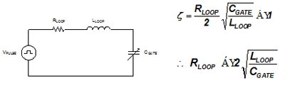
Fig. 6: First order analysis of gate drive circuit
By minimizing LLOOP, the value of RLOOP necessary for critical dampening can be minimized, along with the rise/fall time of the circuit. This can be best accomplished by ensuring that the gate drive is located as closely as possible to the SiC MOSFET.
A Kelvin connection (see Fig. 7 ) for the gate drive is necessary to eliminate stray common mode source inductance, which can result in dynamic source generation. Rapid di/dt of the source current during switching can cause a voltage drop across the common mode stray inductance (V = LSTRAY*di/dt), and the resultant source degeneration has the effect of causing oscillation and limiting di/dt capability of the switching device.
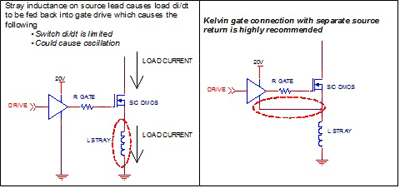
Fig. 7: Gate-drive Kelvin connection
To illustrate the advantages of SiC MOSFETs in power electronics, consider the following solar power inverter application. The test system shown below was developed by the Franhofer Institute [3] — a three-phase, grid-connected solar inverter, rated at 7 kW operating at 16.6 kHz. The B6 topology employs a split-link dc-capacitor with the neutral conductor of each capacitor connected at the center point, with the unit connected to a 400-V grid. The 1,200-V silicon IGBTs originally designed into the system were directly replaced with 1,200-V SiC MOSFETs, without any optimization of the drive circuit. As shown in Fig. 8 , the result was a dramatic increase in system efficiency.
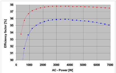
Fig. 8: Comparison of three-phase PV inverter efficiency
Replacement of the silicon IGBTs with SiC MOSFETs achieved the system’s maximum efficiency by 1.92% and boosted the overall European efficiency rating by 2.36%, translating into a 50% reduction in overall system losses and a reduction in heatsink temperature by 43C. According to follow-on research conducted by the Insitut für Solare Energieversorgungstechnik) ISET & SMA GmbH, the three-phase grid-connected system achieved a 99% maximum rating.[5]
To demonstrate the potential for SiC MOSFETs in motor drive applications, engineers at Cree [6] performed an experiment by substituting SiC MOSFETs for the original silicon IGBTs in a 230-Vac, 2-kW three-phase motor drive operating at 16 kHz. The SiC MOSFETs produced a 2% overall efficiency improvement and a 50% reduction in heatsink temperature, enabling a significant reduction and/or simplification of thermal management systems, such as fans. In addition, the ability to operate at higher frequencies (48 kHz and higher), allowed for dramatically reducing the size and weight of magnetic components such as EMI filters and inductors.
For applications in three-phase 480-V power factor correction circuits requiring 1,200-V switching devices, SiC MOSFETs are expected to find wide application. At these voltages, traditional silicon MOSFETs have excessive conduction losses, and silicon IGBTs exhibit significantly higher switching losses, thus putting a limit on their operating frequency. The SiC MOSFETs, however, exhibit both low switching losses and low conduction losses, making them ideal for these types of applications. An added benefit is their overall system efficiency improvement, the capability of higher frequency operation and the reduction in size of inductive and filtering components.
High voltage industrial equipment, including plasma cutters and welders will also be prime applications for the 1,200-V SiC MOSFET. Because of their high frequency operating capability, the SiC MOSFETs enable the use of simple two-level hard switched topologies. By contrast, to operate conventional silicon IGBTs at frequencies of 24 kHz and above typically required a resonant topology with additional components and higher transformer rms currents-per-unit of output power. Alternatively, a multi-level topology utilizing lower voltage silicon MOSFETs can be used; however, this requires a doubling of the number of switches required. By using the SiC MOSFETs, a 10-kW, 1-kV dc/dc converter operating at 32 kHz has been demonstrated with an efficiency of more than 97%.[7]
The commercialization of SiC technology for switching devices represents a revolutionary change in the field of power electronics. Although the cost of a SiC MOSFET, on a device-to-device basis, is higher than that of conventional silicon MOSFETs or IGBTs, the overall system impact of adopting SiC devices must be considered in assessing the full potential for cost savings and the overall value proposition of SiC technology. Beyond the device costs, the following system considerations need to be evaluated for a true picture of the potential cost savings:
1. Passive component reduction
Because of their relative numbers, passive power components often comprise the majority of the overall bill of materials costs in a power electronics application. By increasing the operating frequency, both the number of these components (and their corresponding size and cost) can be reduced.
2. Cooling requirement reduction
By reducing heatsink temperatures by more than 50% (as demonstrated by experiments presented in this article), the adoption of SiC technology has the potential to significantly reduce the size and number of heatsinks, as well as a reduction or elimination of cooling fans.
3. Energy cost reduction over the equipment lifecycle
Looking beyond the simple component costs and manufacturing expenses of a system, the true value proposition of SiC technology comes only if the overall energy savings over the lifecycle of the equipment is considered; and in some cases can be the majority of the savings potential. In systems such as a solar inverter, where cost savings are directly dependent on inverter technology, the elimination of 40% to 50% of switching losses can be the determining factor in the adoption of SiC technology. ■
References:
[1] B. Ozpineci and L. M. Tolbert, “Comparison of Wide Bandgap Semiconductors for Power Electronics Applications,” Oak Ridge National Laboratory, Report ORNL/TM-2003/257, http://www.ornl.gov/~webworks/cppr/y2001/rpt/118817.pdf
[2] R. J. Callanan, A. Agarwal, A. Burk, M. Das, B. Hull, F. Husna, A. Powell, J. Richmond, Sei-Hyung Ryu, and Q. Zhang, “Recent Progress in SiC DMOSFETs and JBS Diodes at Cree,” IEEE Industrial Electronics 34th Annual Conference — IECON 2008, pp 2885 – 2890, 10 – 13 Nov. 2008,
[3] Bob Callanan, “Application Considerations for Silicon Carbide MOSFETs,” Power Electronics Europe, Issue 3, April 2010, pp. 40-43.
[4] B. Burger, D. Kranzer, O. Stalter, S Lehrmann., “Silicon Carbide (SiC) D-MOS for Grid-Feeding Solar-Inverters,” EPE 2007, Aalborg, Denmark. September 2007.
[5] Institut Fur Solare Energieversorgunstechnik – ISET Press release – 23rd Symposium, Photovoltaic Solar Energy, Mar. 6th 2008, Bad Staffelstein, Germany. www.iset.unikassel.de/public/ISET_Pressemitt_Staffelstein_2008_SiC.pdf
[6] Cree, Inc., 4600 Silicon Drive, Durham, NC 27703
[7] Bob Callanan, “Characteristics, Application, and High Power Demonstration of 1.7kV 100 mΩ Silicon Carbide MOSFETs,” to be presented at APEC 2011, Dallas TX.
Advertisement
Learn more about Cree


