Simplifying efficient solid-state backlight driver design
Improved backlight design for longer battery life and better efficiency
JON MARTIS
Microchip Technology
Chandler, AZ
http:\www.microchip.com
Today’s portable electronic devices (cell phones, PDAs, digital music players, etc.) all require some type of backlighting to improve the consumer’s experience. Battery life is always a concern for these devices, and backlighting can be the most energy-depleting feature. Efficiency is the key ingredient for improved battery life, and adding intelligence to the driver circuit can improve the robustness, reliability and efficiency of solid-state backlights in portable electronic devices.
Fig. 1. A PWM boost controller simplifies backlight designs
Efficiency of the backlight design is often equated to design complexity. However, this is not necessarily true. A simple boost circuit can be implemented, using a PWM boost controller that only requires a few external components. Knowing the specifications of the device’s backlight and power source provides the primary information required to determine the values of the external components. The values are determined by applying a few equations to the backlight and product specifications. With this design approach, backlight efficiency exceeding 90% can be achieved.
Microchip’s MCP1650 is a simple PWM Boost controller that has an integrated 750-kHz hysteretic gated oscillator, which allows a high switching frequency that reduces the size of the external inductor and capacitor (see Fig. 1) . Low-resistance internal MOSFETs enable the direct drive of an external switch. Hysteretic operation eliminates the use of compensation components for stable regulation of the circuit output.
The boost controller monitors the voltage at the feedback (FB) pin and overrides the PWM duty cycle output on the EXT pin, shutting down the output when necessary to maintain a constant current in the feedback resistor.
Backlight app design
Let’s apply the above scenario to a backlight application design. The portable product for our example design includes four LEDs ( If = 20 mA / Vf = 3.6 V) that provide backlighting powered by a 3.7-V Li-polymer battery.
We now have all the information required to start the design.
The schematic components required for this efficient Boost circuit are (also see Figure 2 ):
L1 – Inductor – Boost energy storage
Q1 – MOSFET – Boost circuit switch
D1 – Diode, fast switching – Boost diode
R1 – Resistor – feedback voltage, sets forward current
C1 – Capacitor – voltage output stability
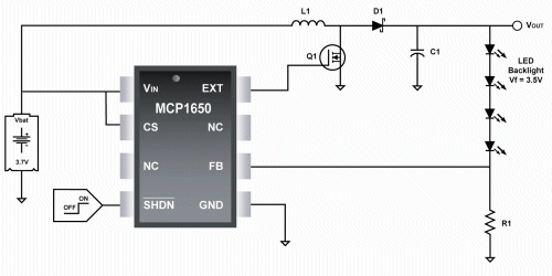
Fig. 2. A simple boost circuit can be implemented using a PWM boost controller that only requires a few external components.
Sizing these components is the challenge! Taken one at time, this challenge is quickly overcome. The feedback voltage for the hysteric controller regulates the PWM output, by comparing the voltage at the FB pin to an internal 1.22-V reference. The feedback resistor therefore, determines the current that will be regulated through the LEDs (20 mA). R1 is determined using Ohm’s Law—V = IR; R1 = V(FB)/If —and the power equation: P = V x I; P(R1) = V(FB) x If. These equations utilize the following values:
R1 = 61 Ω = (1.22 V/20 mA)
P(R1) = 24 mW = 1.22 V x 20 mA
Since 61 Ω is not a standard value, 62 Ω will be used—producing a forward current of 19.7 mA, which is very close to the 20-mA target. Next, we need to determine the voltage output (Vout), the maximum output power, P(out) and the input power P(in), in order to determine the inductor value.
Vout is defined by the forward voltage of the four LEDs and the feedback voltage from the current-sense resistor: Vout = 4 x Vf + Vfb. From the information provided and the Vfb from the MCP1650 Datasheet, we can ascertain the following values:
Vout = 15.62 V = (4 x 3.6 V) + 1.22 V
P(out) is the output voltage times the LED forward current; P(out) = Vout x If. Thus, we get:
P(out) = 312 mW = 15.62 V x 20 mA
Determining the power input requires us to choose a ballpark efficiency for our circuit. Being conservative, we can estimate that the efficiency is about 80%. (In similar designs, the efficiency has been measured at 95%, using this same design method.) P(in) becomes a function of the output power and the estimated efficiency:
P(in) = P(out)/ efficiency.
P(in) = 390 mW = (312 mW/0.8)
The PWM boost controller operates at a fixed 80% duty cycle, when V(in) is less than 3.8 V. The maximum voltage boost, while operating in a continuous inductor-current mode, is five times the input voltage. Boost is determined by the equation 1/(1-Duty Cycle). A fully charged battery can boost to 18.5 V, about 1.8 V higher than needed to sustain the 20-mA constant current. When the battery voltage decays to about 3.2 V, a continuous-current-mode design will not deliver the power required to maintain the current drive. Li-polymer batteries typically should not be depleted below 3.0 V, meaning the operating voltage is 3.7 V
Designing for discontinuous inductor-current mode allows higher boost, but also increases peak inductor current, I(pk). Operating in this mode, we must store enough energy in the inductor during the duty cycle “off time” to handle the energy demand during the “on time.” This means that the energy stored in the inductor must be capable of producing more power than the P(in) value (390 mW), calculated earlier. To size the inductor, the following two equations will be used:
1. I(pk) = (V(in)/L ) x T(on)
Note: T(on) = Time x Duty Cycle, (1/750 kHz) x 80% =1.07 µS
2. Energy = 1/2 x L * I(pk)2
In the equations, I(pk) and L are unknown. By selecting a standard inductor value, a starting point can be established. The final value can be identified by repeating the calculations. A spreadsheet is extremely handy, and makes the inductor selection almost painless. Not knowing where to start with an inductor value, 3.3 µH is selected. Plugging it into the equations yields:
• I(pk) = 0.97A = (3.0 V/ 3.3 µH) x 1.07 µsS
• Energy = 1.55 µJ = 1/2 x 3.3 µH * (0.97)2
Now, determining the power, (Power = Energy/Time):
• Power(3.3 µH) = 1.165 W or(J/s) = 1.55 µJ / 1.33 µs
The power calculated, due to a 3.3-µH inductor, is nearly four times larger than needed for the power input requirement of P(in) = 390 mW. Using a spreadsheet reveals that a 9.1-µH inductor will provide enough power. The advantage of increasing the inductor value is that peak current is significantly reduced, requiring a smaller-diameter inductor wire and, therefore, a smaller inductor package.
Working through the equations:
• I(pk) = 0.352 A = (3.0 V/ 9.1 µH) x 1.07 µs
• Energy = 0.563 µJ = 1/2 * 9.1 µH * (0.352)2
• Power(3.3 µH) = 0.422 W or (J/s) = 0.563 µJ / 1.33 µs
This defines the inductor specification as 9.1 µH, with a minimum peak-current rating of 352 mA.
Take a breath and relax. We have overcome the greatest part of our design challenge. The remainder of the design becomes a search through datasheets to select the other components.
Continuing to define the components, the MOSFET switch needs to have a drain-to-source voltage rating greater than V(out), plus some margin (10%-20% will be sufficient). Additionally, the MOSFET should have a logic-level gate threshold voltage and a low RDS value — the lower the better.
The boost diode will be switching on and off at the gated oscillator frequency of 750 kHz. Schottky diodes do a great job, having very fast switching characteristics and a low forward-drop, which reduces losses and improves system efficiency.
The output capacitor, C1, can be a ceramic or ESR tantalum capacitor. Typically, lower values are less expensive and smaller. However, they produce a higher output ripple voltage. Thus, a 10-µF, 50-V capacitor will be good.
The final components are defined as:
L1 – Inductor – 9.1 µH, Ipk > 352 mA
Q1 – MOSFET – IPK > 353 mA; VDS > 19 V; 3.7 V > VGS >3.0 V
D1 – Diode – VR > 20 V; IO > 352 mA; trr
R1 – Resistor – 62 Ω, 1/10 W
C1 – Capacitor – 10 µF / 50 V
The /SHDN pin controls the output of the EXT pin to the MOSFET switch. This pin can be controlled through an external signal to enable the output. Enhancements to the driver circuit’s function and performance can easily be realized, by adding an inexpensive 6-pin microcontroller. These enhancements can include dimming control, thermal management, battery voltage monitoring and other advanced features under software control, increasing the reliability and battery life of the device.
A PWM boost controller simplifies backlight design, using hysteretic control to manage the PWM duty cycle and system regulation. This method of design eliminates the need for additional compensation components and calibration. LED backlight current regulation and controller stability are a function of the feedback resistor, R1. Selection of an inductor for a Boost circuit can be a difficult task. Defining a few parameters of the circuit, such as voltage output and LED current, reduces this task to solving a few equations and selecting components from datasheets.
Advertisement
Learn more about Microchip Technology


