Distributed systems dealing with large currents can have their “common” ground reference see substantial local variations. In automotive electronics, for instance, electric motors during cold crank produce large ground offset noise. The technique of simulating ground offset to test automotive electronic systems will help developers ensure system reliability.
In a distributed system, each electronic subsystem must able to communicate with the others reliably, even in the presence of substantial noise. High-current-handling systems, such as automotive electronics, face a special challenge: the presence of large ground offset noise. In such systems, the ground current can be up to 100 A or more and often are transient in nature; i.e., they last for a short duration. During this transient current, because ground wires and planes always have some parasitic resistance, the current will cause a sizable IR voltage drop across the wire. This IR voltage means that there will be a ground reference difference between communication systems.
Ground offset
As shown in Fig. 1 , the high current source (i.e., 12-V lead-acid battery) outputs very high current in the orders of hundreds of amperes to the load (i.e., cranking motor). This current is returned through the ground wire or chassis, which has low, but not zero, resistance. Even with a 10-mΩ ground resistance, the 100 A will result in a 1-V difference between two different locations in the ground plane.
Because the car’s communication subsystems connect to the same ground node, but at different points, there can be as much as a 1-V difference between the ground references of the transmitter and receiver units. That is, GND-R is 1 V higher than GND-T. These communication systems must, therefore, be designed to handle such a difference and they must be thoroughly tested during development.
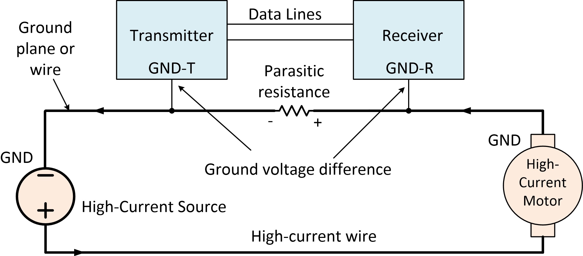
Fig. 1: Ground offset voltage is caused by high current in ground plane.
To help further understand the ground offset voltage effect, Fig. 2 shows the equivalent circuit of Fig. 1 with the 1-V IR drop when there is a 100-A ground current. This voltage is in between the two communication subsystems. This offset voltage causes the two communication subsystems ground inputs at a different voltage level. If the ground voltage difference is large enough, communication could fail. To verify that a design will work reliably, then, it must be tested with subsystems operating with ground reference offsets.

Fig. 2: Simplified equivalent circuit of Fig. 1. There is a ground offset voltage in between the two communication subsystems.
Ground offset simulation and generation
During product development phase, it is much more convenient to simulate the ground offset when testing the communication system than pumping 100 A. One way to do so, as shown in Fig. 3 , is to simulate the ground offset voltage with a four-quadrant power supply, such as the Accel TS200 or TS250, inserted between the transmitter ground (GND-T) and the receiver ground nodes.

Fig. 3: A four-quadrant power supply can help simulate offset ground voltage.
Understanding four-quadrant power supply
A four-quadrant power supply is a special voltage supply that can both sink or source current, regardless of whether the output voltage is positive or negative. In contrast, a regular power supply can only source current; it cannot sink current. To further understand four-quadrant power supply, Fig. 4 shows the four-quadrant diagram.

Fig. 4: Diagram showing a voltage supply operating in each of the four quadrants.
In the first quadrant, the voltage is positive and the current is also positive (sourcing current). In the second quadrant, the output voltage is negative, but the current is still positive (sourcing). In the third quadrant, the voltage is negative and the current is sinking. And finally, the fourth quadrant is negative voltage but sourcing current. The typical lab power supply can only operate in the first quadrant.

Fig. 5: Modulated power supply is used for ground offset testing.
DC ground offset testing
For ground offset voltage simulation as shown in Fig. 3 , testers usually use the second and the fourth quadrant. Two test cases are needed for testing the transceivers. The first test case has the receiver use the higher ground voltage. To achieve this, testers should set the four-quadrant voltage supply to positive voltage. The second case is when the transmitter has the higher ground voltage. In this second case, the power supply should be set to negative voltage (and sourcing current). For maximum confidence in the system’s reliability, the transceiver must be thoroughly tested with different ground offset levels, both positive and negative voltages.
Here is the recommended test procedure:
1. Connect the supply’s positive output terminal to the transmitter’s GND-T node.
2. Connect the negative output terminal to a common ground.
3. Connect the receiver ground (GND-R) to the common ground.
4. Initially set the supply output to zero volts.
5. Test the communication systems.
6. Increase the output voltage to a higher voltage (i.e., +100 mV).
7. Repeat Steps 5 and 6 until communications fail. This is the system’s failure point.
8. Repeat Steps 1 through 7 for using negative offset voltage steps.
AC ground offset testing
Such ground offsets may not only be DC voltages but are often AC or transient in nature. Transient ground offsets occur, for instance, when large surges of current get injected into the ground plane. This surge will cause the ground to bounce, acting like a noise source that increases the overall system noise level. This can affect more than the communications subsystems. For example, large ground noise will reduce the signal-to-noise ratio in analog and ADC/DAC circuits or increase the jitter level in digital systems as well as corrupt communications integrity.
It is, therefore, important to thoroughly test all subsystems and circuits that are exposed to high-level ground noise. The easiest way to simulate transient noise is to use an AC four-quadrant power supply, such as the Accel TS250 waveform amplifier. Fig. 6 shows the test setup. a signal generator produces the noise or transient. The waveform amplifier (which can also work as a four-quadrant power supply) acts like a buffer that, due to its very low output impedance, can sink or source large currents.

Fig. 6: Test setup generating ground noise to simulate large ground transient current.
Conclusion
A four-quadrant voltage supply is crucial to simulate ground offset voltages that mimic ground plane voltage difference in a high current system. Furthermore, the simulated offset voltage supply must be able to both sink and source current. Such simulation is needed to thoroughly test all of the subsystems (transceivers) in electronic products that handle large currents.
Advertisement
Learn more about Electronic Products Digital


