Simulation technique for optimizing white-LED design
Emerging innovations produce better designs, optimization, and failure analysis
BY RICARDO BORGES, WEI-CHOON NG, and GERGO LETAY
Synopsys
Mountain View, CA
http://www.synopsys.com
White light-emitting diodes (LEDs) are currently a source of great research and commercial interest in view of the revolutionary energy-efficiency and cost-savings potential offered by solid-state lighting. Amid a plethora of design possibilities, the most promising and cost-effective approach to producing white light is via spectral conversion of blue LED emissions using a luminescent material that encapsulates the entire LED structure.
The preferred luminescent material is phosphor and its composite due to their high spectral conversion efficiency. As white-LED designs are refined in research labs and make their way into commercial markets, the need for simulation tools to aid in the design and optimization of these promising devices is emerging. Why simulate white LEDs?
LEDs are highly sophisticated optoelectronic devices. The pressing design task is to map a host of design parameters to desired output characteristics. This mapping is not direct, and the design parameters are intimately coupled to one another in a nonlinear fashion. Therefore, the designer faces enormous difficulties in correlating design parameters (such as thickness of epitaxial layers, doping distribution, quantum-well composition, electrode patterning and 3-D structural shape) to output characteristics, such as radiation spectrum (color rendering), high brightness, operating-temperature range, wall-plug efficiency, internal quantum efficiency, lifetime, and radiation pattern. A design optimized to these attributes can command a premium in a highly competitive commercial environment.
Device simulation rapidly helps to unravel failures and inadequacies of the LED design by showing current crowding and spreading, recombination traps, and design flaws that are not apparent or cannot be measured by experiment (either directly or indirectly). Moreover, after the device structure is optimized, simulation lends itself to an examination of the sensitivity of output characteristics to the device structure, thereby providing a design-for-manufacturing (DFM) framework for LEDs.
Simulator requirements
The development of a simulator for white-LED design and optimization must cover a range of electrical and optical phenomena. The electrical transport of holes and electrons requires the coupled solution of the Poisson, continuity, and thermal equations, together with associated mobility, recombination, and generation models, and special treatment of carrier scattering into the quantum wells (QWs). The photon production (spontaneous emission) and amplification (stimulated emission) processes within the QWs are carefully treated using advanced gain calculations. Blue-light emission necessitates the use of indium gallium nitride/gallium nitride (InGaN/GaN) QWs, and these further require the inclusion of polarization charge sheets and piezoelectric screening effects. These electrical transport simulations must then be intricately coupled to the optical domain.
Due to the relatively large dimensions of LEDs (a few hundred microns across), ray optics approaches such as ray tracing are typically employed and accepted as valid optical solutions. Using a spectrally resolved ray tracing (proprietary to Synopsys) allows spontaneous emission spectra to be embedded in the simulations and then evolved as the rays traverse regions of stimulated gain, absorption, and luminescence. There are four possible spectral-evolution processes:
Part of the spontaneous spectrum is amplified by stimulated emission in the QWs—this is a carrier recombination process.Part of the spontaneous spectrum is absorbed to generate electron-hole pairs to be subjected to electrical transport—this is a carrier generation process.Part of the absorbed spectrum is instantaneously re-emitted, thereby modifying the emission isotropy of that active cell.Part of the spectrum is spectrally converted in the luminescent region.
These spectral-evolution processes consequently give rise to a modified spontaneous-emission spectrum. The first three processes constitute a novel photon-recycling model that includes amplified spontaneous emission. Since brighter LEDs require higher-current injection, the active region (QWs) is pumped with enough carriers for stimulated emission to occur. Stimulated emission will amplify the spontaneous emission spectrum, giving rise to amplified spontaneous emission (ASE). Although ASE has been studied extensively in resonating structures such as lasers, optical amplifiers, resonant-cavity LED (RCLED) and super-luminescent LED (SLED), the inclusion of ASE in the non-resonant structures typical in modern white-LED design has not been fully explored, and is now enabled by this novel photon-recycling model.
The photons production/absorption and carrier recombination/generation are carefully balanced to ensure particle conservation when a net photon recycling recombination rate is fed back into the continuity equations. This enables the important physical effects in white-LED structures to be captured in a fully coupled and self-consistent electro-opto-thermal simulation.
Simulation of a 3-D ATON white LED
To illustrate the techniques discussed in the previous section, let’s look at the simulation results of a 3-D ATON white LED using the Sentaurus Device simulator from Synopsys. Figure 1 shows two simplified 3-D ATON structures that are encased in luminescent material.
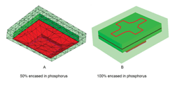
Fig. 1. Simplified 3-D ATON structures are encased in luminescent material, about 50% covered with phosphor (a) and totally covered (b).
Figure 1(a) is about 50% covered with phosphor, while Fig. 1(b) is totally covered. The top electrode is a cross pattern to facilitate current spreading without over-blocking the top-surface light extraction, and the bottom electrode covers the entire base. The LED structure contains two InGaN/GaN QWs designed to have peak spontaneous emissions at around 460 nm. The substrate is silicon carbide (SiC) and the buffer layers are aluminum gallium nitride (AlGaN)
Figure 2 shows the current spreading and temperature profiles, both of which are not directly measurable and add key physical insight. Good current spreading is essential to reducing photon absorption by the QWs. On the other hand, current spreading also affects the way that heat production is distributed via the Joule heating and recombination processes, and it becomes a design issue to simultaneously minimize both absorption and temperature rise.
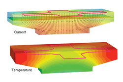
Fig. 2. Good current spreading is essential to reducing photon absorption by the active region.
The output spectra of both devices are shown in Fig. 3 , which shows that blue emissions from the InGaN/GaN QWs were spectrally converted successfully. This particular simulation used a simple phosphor with an absorption peak at 460 nm and emission peak at 560 nm.
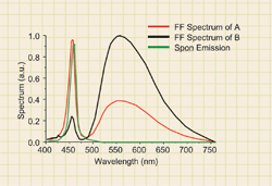
Fig. 3. The output spectra of both devices show that blue emissions from the InGaN/GaN QWs were spectrally converted successfully.
The measured output power is a product of the extraction efficiency and the total power. LED extraction efficiency is generally low, implying that most of the light is trapped within the device. However, a properly designed ATON structure can exceed 50% extraction efficiency, providing a strong motivation for simulation studies. The trapped light undergoes spectral evolution as it traverses active QWs and luminescent regions multiple times in succession.
Advertisement
Learn more about Synopsys


