By Jean-Jacques DeLisle, contributing writer
In order to usher in the next generation of high-definition display technology, a research team from the Department of Energy’s Lawrence Berkeley National Laboratory (Berkeley Lab) has developed new light-emitting nanowire technology built from soft semiconductors. From a single nanowire, the team was able to develop red, green, blue (RGB) light emitters and nanowires down to 500 nanometers. To give a comparison, Apple’s flagship retina displays can reach to about 400 pixels per inch, at roughly 60 micrometers per pixel. Berkeley Lab researchers were able to make light emitters that could reach roughly 50.000 pixels per inch, over two orders of magnitude greater.
At this size, this new technology could compete with the latest quantum dot technology, which still uses standard semiconductor nanocrystals that emit light. Though the research demonstration focused on light emission, the “soft” semiconductor nanowire heterojunction device technology may be useful for more than just display applications and could be a major player in future photovoltaic, solid-state lighting, multicolor LED lasers, and other cutting-edge optoelectronic applications. Moreover, this same technology may also be viable in high-density diodes and transistor arrays, opening the doors to many beyond state-of-the-art applications.
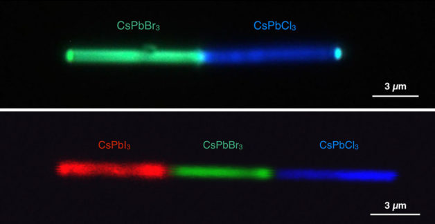
This graphic compares the color generation from a cesium lead bromide (CsPbBr3 )-cesium lead chloride (CsPbCl3 ) heterojunction semiconductor (Top Panel) under UV excitation, and cesium lead iodide (CsPbI3 )-cesium lead bromide-cesium lead chloride (Bottom Panel) red, blue, and green configuration under UV excitation. Credit: Letian Dou/Berkeley Lab and Connor G. Bischak/UC Berkeley.
The backbone of this new technology is the use of halide perovskite nanowire heterojunctions, which is made up of a lattice structure of ionic, rather than covalent, bonds like traditional semiconductors. Dubbed “soft” semiconductors, ionic bonds are more easily manipulated than “harder” covalent bonds.
In the report published on pnas.org, Peidong Yang, senior faculty scientist at Berkeley Lab’s Materials Sciences Division, said, “With inorganic halide perovskite, we can easily swap the anions in the ionic bonds while maintaining the single crystalline nature of the materials. This allows us to easily reconfigure the structure and composition of the material. That’s why halide perovskites are considered soft lattice semiconductors. Covalent bonds, in contrast, are relatively robust and require more energy to change. Our study basically showed that we can pretty much change the composition of any segment of this soft semiconductor.”
This means that researchers were able to employ nanofabrication techniques with anion exchange chemistry to swap the halide ions of cesium lead halide perovskite to either cesium bromide or cesium chloride, thus changing the color emission. The special chemical soak required to swap the anions can also be done at standard laboratory room temperature and doesn’t require the precision high-temperature thermal control and vacuum environmental that other semiconductor processing requires.
“It’s a simple process, and it is very easy to scale up,” said Yang. “You don’t need to spend long hours in a clean room, and you don’t need high temperatures.”
Important aspects of this discovery are that the researchers claim that they are able to “tune” the materials throughout the entire visible light spectrum and, maybe most importantly, that the processing for this technology may be much simpler than with standard colloidal semiconductors. This could imply that these soft semiconductors could be manufactured with comparably higher yields with less processing steps, which could amount to lower costs and less waste.
“For conventional semiconductors, fabricating the junction is quite complicated and expensive,” said postdoctoral fellow in Yang’s lab and study, co-lead author Letian Dou, in the report. “High temperatures and vacuum conditions are usually involved to control the materials’ growth and doping. Precisely controlling the materials composition and property is also challenging because conventional semiconductors are hard due to strong covalent bonding.”
Though the material still requires much development, which includes improved resolution and integration/characterization as components in electrical circuits, the material shows early promise. This method is also competing against many highly publicized, researched, and incumbent technologies. If the material can even offer comparable display, diode, and transistor performance than current technologies, but provide higher yields and lower processing costs, soft semiconductors with halide perovskite heterojunctions may find their way into future smartphones, smartwatches, augmented reality, and virtual reality display technology along with many other lighting and electronic applications.
Advertisement
Learn more about Electronic Products Magazine


